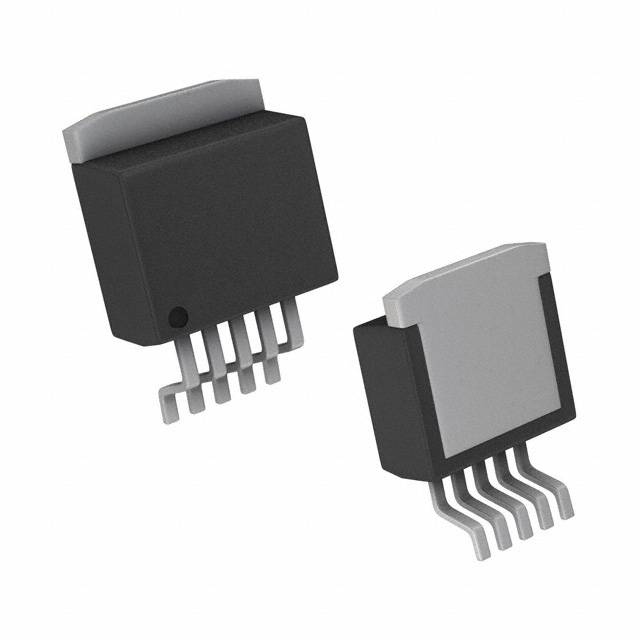
TPS75533KTTT
ObsoleteLDO REGULATOR POS 3.3V 5A 6-PIN(5+TAB) DDPAK T/R
Deep-Dive with AI
Search across all available documentation for this part.

TPS75533KTTT
ObsoleteLDO REGULATOR POS 3.3V 5A 6-PIN(5+TAB) DDPAK T/R
Deep-Dive with AI
Technical Specifications
Parameters and characteristics for this part
| Specification | TPS75533KTTT |
|---|---|
| Control Features | Enable, Power Good |
| Current - Output | 5 A |
| Current - Quiescent (Iq) | 200 µA |
| Mounting Type | Surface Mount |
| Number of Regulators | 1 |
| Operating Temperature [Max] | 125 °C |
| Operating Temperature [Min] | -40 °C |
| Output Configuration | Positive |
| Output Type | 1.81 mOhm |
| Package / Case | TO-263-6, TO-263BA, D2PAK (5 Leads + Tab) |
| Protection Features | Over Temperature, Over Current, Under Voltage Lockout (UVLO), Reverse Polarity |
| PSRR | 60 dB |
| Supplier Device Package | TO-263 (DDPAK-5) |
| Voltage - Input (Max) [Max] | 5.5 V |
| Voltage - Output (Min/Fixed) | 3.3 V |
| Voltage Dropout (Max) [Max] | 0.5 V |
Pricing
Prices provided here are for design reference only. For realtime values and availability, please visit the distributors directly
| Distributor | Package | Quantity | $ | |
|---|---|---|---|---|
Description
General part information
TPS75501 Series
The TPS755xx family of 5-A low dropout (LDO) regulators contains four fixed voltage option regulators with integrated power-good (PG\) and an adjustable voltage option regulator. These devices are capable of supplying 5 A of output current with a dropout of 250 mV (TPS75533). Therefore, the device is capable of performing a 3.3-V to 2.5-V conversion. Quiescent current is 125 uA at full load and drops down to less than 1 uA when the device is disabled. The TPS755xx is designed to have fast transient response for large load current changes.
Because the PMOS device behaves as a low-value resistor, the dropout voltage is very low (typically 250 mV at an output current of 5 A for the TPS75533) and is directly proportional to the output current. Additionally, since the PMOS pass element is a voltage-driven device, the quiescent current is very low and independent of output loading (typically 125 uA over the full range of output current). These two key specifications yield a significant improvement in operating life for battery-powered systems.
The device is enabled when EN\ is connected to a low-level voltage. This LDO family also features a sleep mode; applying a TTL high signal to EN\ (enable) shuts down the regulator, reducing the quiescent current to less than 1 uA at TJ= 25°C. The power-good terminal (PG\) is an active low, open drain output, which can be used to implement a power-on reset or a low-battery indicator.
Documents
Technical documentation and resources


