Deep-Dive with AI
Search across all available documentation for this part.

Deep-Dive with AI
Technical Specifications
Parameters and characteristics for this part
| Specification | DS3486MX/NOPB |
|---|---|
| Mounting Type | Surface Mount |
| Number of Drivers/Receivers [custom] | 0 |
| Number of Drivers/Receivers [custom] | 4 |
| Operating Temperature [Max] | 70 °C |
| Operating Temperature [Min] | 0 °C |
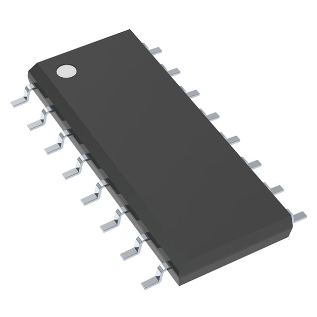
| Package / Case | 16-SOIC |
| Package / Case [x] | 0.154 in |
| Package / Case [y] | 3.9 mm |
| Protocol | RS423, RS422 |
| Receiver Hysteresis | 140 mV |
| Supplier Device Package | 16-SOIC |
| Type | Receiver |
| Voltage - Supply [Max] | 5.25 V |
| Voltage - Supply [Min] | 4.75 V |
Pricing
Prices provided here are for design reference only. For realtime values and availability, please visit the distributors directly
| Distributor | Package | Quantity | $ | |
|---|---|---|---|---|
| Digikey | Cut Tape (CT) | 1 | $ 1.40 | |
| 10 | $ 1.25 | |||
| 25 | $ 1.19 | |||
| 100 | $ 0.98 | |||
| 250 | $ 0.91 | |||
| 500 | $ 0.81 | |||
| 1000 | $ 0.64 | |||
| Digi-Reel® | 1 | $ 1.40 | ||
| 10 | $ 1.25 | |||
| 25 | $ 1.19 | |||
| 100 | $ 0.98 | |||
| 250 | $ 0.91 | |||
| 500 | $ 0.81 | |||
| 1000 | $ 0.64 | |||
| Tape & Reel (TR) | 2500 | $ 0.59 | ||
| 5000 | $ 0.56 | |||
| 12500 | $ 0.54 | |||
Description
General part information
DS3486 Series
Texas Instruments' quad RS-422, RS-423 receiver features four independent receivers which comply with EIA Standards for the electrical characteristics of balanced/unbalanced voltage digital interface circuits. Receiver outputs are 74LS compatible, TRI-STATE structures which are forced to a high impedance state when the appropriate output control pin reaches a logic zero condition. A PNP device buffers each output control pin to assure minimum loading for either logic one or logic zero inputs. In addition, each receiver has internal hysteresis circuitry to improve noise margin and discourage output instability for slowly changing input waveforms.
Texas Instruments' quad RS-422, RS-423 receiver features four independent receivers which comply with EIA Standards for the electrical characteristics of balanced/unbalanced voltage digital interface circuits. Receiver outputs are 74LS compatible, TRI-STATE structures which are forced to a high impedance state when the appropriate output control pin reaches a logic zero condition. A PNP device buffers each output control pin to assure minimum loading for either logic one or logic zero inputs. In addition, each receiver has internal hysteresis circuitry to improve noise margin and discourage output instability for slowly changing input waveforms.
Documents
Technical documentation and resources


