Zenode.ai Logo
Beta
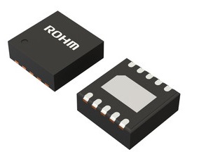
Product thumbnail image
Integrated Circuits (ICs)

BDL00A5NUF-CE2

Active
Rohm Semiconductor

AUTOMOTIVE 500MA, ADJUSTABLE OUTPUT LDO REGULATOR

Deep-Dive with AI

Search across all available documentation for this part.

Product thumbnail image
Integrated Circuits (ICs)

BDL00A5NUF-CE2

Active
Rohm Semiconductor

AUTOMOTIVE 500MA, ADJUSTABLE OUTPUT LDO REGULATOR

Technical Specifications

Parameters and characteristics for this part

SpecificationBDL00A5NUF-CE2
Control FeaturesEnable
Current - Output500 mA
Current - Quiescent (Iq)65 µA
GradeAutomotive
Mounting TypeWettable Flank, Surface Mount
Number of Regulators1
Operating Temperature [Max]150 °C
Operating Temperature [Min]-40 °C
Output ConfigurationPositive
Output TypeAdjustable
Package / Case10-VFDFN Exposed Pad
Protection FeaturesOver Temperature, Over Current, Short Circuit
PSRR65 dB
QualificationAEC-Q100
Supplier Device PackageVSON10FV3030
Voltage - Input (Max) [Max]18 V
Voltage - Output (Max) [Max]17 V
Voltage - Output (Min/Fixed)1 V
Voltage Dropout (Max) [Max]0.6 V

Pricing

Prices provided here are for design reference only. For realtime values and availability, please visit the distributors directly

DistributorPackageQuantity$
DigikeyN/A 2970$ 1.10

Description

General part information

BDL00A5NUF-C Series

The BDL00A5NUF-C is a linear regulator designed as a low current consumption product for power supplies in various automotive applications. This product is designed for up to 20V as an absolute maximum voltage and to operate until 500mA for the output current with low current consumption 30µA (Typ). The reference voltage accuracy (ADJ pin voltage accuracy) is a very high accuracy (The tolerance of feedback resistor is not included.), ±2 %. The output voltage can be adjusted between 1V and 17V by an external resistive divider connected to the ADJ pin. The output shutdown function is integrated in the devices. A logical "HIGH" at the EN Pin turns on the device, and in the other side, the device is controlled to disable by a logical "LOW" input to the EN Pin. The device features the integrated Over Current Protection to protect the device from a damage caused by a shortcircuiting or an overload. This product also integrates Thermal Shutdown Protection to avoid the damage by overheating. Furthermore, low ESR ceramic capacitors are sufficiently applicable for the phase compensation.

Documents

Technical documentation and resources

How to Use the Thermal Resistance and Thermal Characteristics Parameters

Thermal Design

Calculating Junction Temperature from Inrush Current

Thermal Design

Table of resistance for output voltage setting on linear regulator Ics

Schematic Design & Verification

How to Select Reverse Current Protection Diodes for LDO Regulators

Schematic Design & Verification

How to Use the Two-Resistor Model

Thermal Design

Two-Resistor Model: BDL00A5NUF-C

Thermal Design

Simple Test Method for Estimating the Stability of Linear Regulators

Schematic Design & Verification

Usage of SPICE Macromodel (for LDO)

Schematic Design & Verification

Connecting LDOs in Parallel

Schematic Design & Verification

Reverse Voltage Protection

Schematic Design & Verification

Precautions When Measuring the Rear of the Package with a Thermocouple

Thermal Design

Factory Information

Manufacturing Data

Impedance Characteristics of Bypass Capacitor

Schematic Design & Verification

Thermal Resistance

Thermal Design

BDL00A5NUF-C Data Sheet

Data Sheet

Problem Situations: Power Supply Does Not Start

Schematic Design & Verification

Design Guide and Example of Stencil for Exposed Pad

Thermal Design

Heat Dissipation Effect of Thermal Via in Exposed Pad Type Package

Thermal Design

Basics of Thermal Resistance and Heat Dissipation

Thermal Design

Measurement Method for Phase Margin with Frequency Response Analyzer (FRA)

Schematic Design & Verification

PCB Layout Thermal Design Guide

Thermal Design

Six Steps for Successful Thermal Design of LDO Regulator ICs

White Paper

What Is Thermal Design

Thermal Design

Power Supply Sequence Circuit with General Purpose Power Supply IC

Schematic Design & Verification

EMC Measures for LDOs

Schematic Design & Verification

θ<sub>JC</sub> and Ψ<sub>JT</sub>

Thermal Design

Method for Calculating Junction Temperature from Transient Thermal Resistance Data

Thermal Design

Basics of Linear Regulators

Schematic Design & Verification

Thermal Calculation for Linear Regulator

Thermal Design

θ<sub>JA</sub> and Ψ<sub>JT</sub>

Thermal Design

VSON10FV3030 Package Information

Package Information

Suppression Method of Switching Noise Using Linear Regulator and Low Pass Filter

Schematic Design & Verification

Five Steps for Successful Thermal Design of IC

White Paper

Overview of ROHM's Simulation Models(for ICs and Discrete Semiconductors)

Technical Article

Judgment Criteria of Thermal Evaluation

Thermal Design

Solder Joint Rate and Thermal Resistance of Exposed Pad

Thermal Design

Power Source ON/OFF Characteristics for Linear Regulator

Schematic Design & Verification