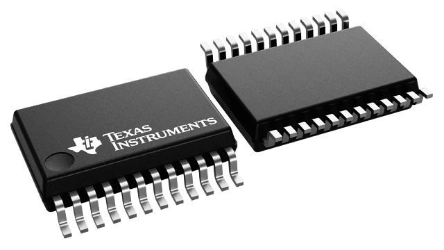
SN74LVC646ADBR
ActiveOCTAL BUS TRANSCEIVER AND REGISTER WITH 3-STATE OUTPUTS
Deep-Dive with AI
Search across all available documentation for this part.

SN74LVC646ADBR
ActiveOCTAL BUS TRANSCEIVER AND REGISTER WITH 3-STATE OUTPUTS
Deep-Dive with AI
Technical Specifications
Parameters and characteristics for this part
| Specification | SN74LVC646ADBR |
|---|---|
| Current - Output High, Low | 24 mA |
| Mounting Type | Surface Mount |
| Number of Bits per Element | 8 |
| Number of Elements | 1 |
| Operating Temperature [Max] | 85 °C |
| Operating Temperature [Min] | -40 °C |
| Output Type | 3-State |
| Package / Case | 24-SSOP |
| Supplier Device Package | 24-SSOP |
| Voltage - Supply [Max] | 3.6 V |
| Voltage - Supply [Min] | 1.65 V |
Pricing
Prices provided here are for design reference only. For realtime values and availability, please visit the distributors directly
| Distributor | Package | Quantity | $ | |
|---|---|---|---|---|
| Digikey | Cut Tape (CT) | 1 | $ 1.64 | |
| Digi-Reel® | 1 | $ 1.64 | ||
| Tape & Reel (TR) | 2000 | $ 0.75 | ||
| 6000 | $ 0.72 | |||
| 10000 | $ 0.69 | |||
| Texas Instruments | LARGE T&R | 1 | $ 1.23 | |
| 100 | $ 1.02 | |||
| 250 | $ 0.73 | |||
| 1000 | $ 0.55 | |||
Description
General part information
SN74LVC646A Series
The SN54LVC646A octal bus transceiver and register is designed for 2.7-V to 3.6-V VCCoperation, and the SN74LVC646A octal bus transceiver and register is designed for 1.65-V to 3.6-V VCCoperation.
These devices consist of bus-transceiver circuits, D-type flip-flops, and control circuitry arranged for multiplexed transmission of data directly from the input bus or from the internal registers. Data on the A or B bus is clocked into the registers on the low-to-high transition of the appropriate clock (CLKAB or CLKBA) input. Figure 1 illustrates the four fundamental bus-management functions that are performed with the ’LVC646A devices.
Output-enable (OE)\ and direction-control (DIR) inputs control the transceiver functions. In the transceiver mode, data present at thehigh-impedance port is stored in either register or in both.
Documents
Technical documentation and resources


