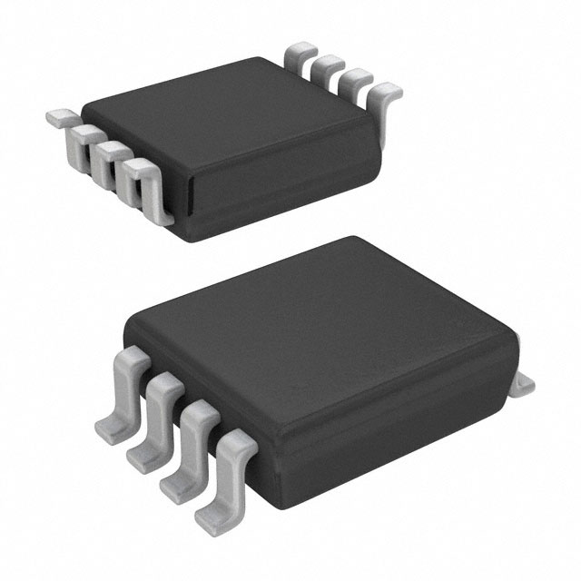
NC7SP74K8X
ObsoleteTINYLOGIC ULP D-TYPE FLIP-FLOP WITH PRESET AND CLEAR
Deep-Dive with AI
Search across all available documentation for this part.

NC7SP74K8X
ObsoleteTINYLOGIC ULP D-TYPE FLIP-FLOP WITH PRESET AND CLEAR
Deep-Dive with AI
Technical Specifications
Parameters and characteristics for this part
| Specification | NC7SP74K8X |
|---|---|
| Clock Frequency | 150 MHz |
| Current - Output High, Low [custom] | 2.6 mA |
| Current - Output High, Low [custom] | 2.6 mA |
| Current - Quiescent (Iq) | 900 nA |
| Function | Reset, Set(Preset) |
| Input Capacitance | 2 pF |
| Max Propagation Delay @ V, Max CL | 8 ns |
| Mounting Type | Surface Mount |
| Number of Bits per Element | 1 |
| Number of Elements | 1 |
| Operating Temperature [Max] | 85 °C |
| Operating Temperature [Min] | -40 °C |
| Output Type | Complementary |
| Package / Case | 8-VFSOP |
| Package / Case [y] | 2.3 mm |
| Package / Case [y] | 0.091 in |
| Supplier Device Package | US8 |
| Trigger Type | Positive Edge |
| Type | D-Type |
| Voltage - Supply [Max] | 3.6 V |
| Voltage - Supply [Min] | 0.9 V |
Pricing
Prices provided here are for design reference only. For realtime values and availability, please visit the distributors directly
| Distributor | Package | Quantity | $ | |
|---|---|---|---|---|
| Digikey | Cut Tape (CT) | 1 | $ 0.83 | |
| 10 | $ 0.48 | |||
| 25 | $ 0.40 | |||
| 100 | $ 0.30 | |||
| 250 | $ 0.26 | |||
| 500 | $ 0.23 | |||
| 1000 | $ 0.21 | |||
| Digi-Reel® | 1 | $ 0.83 | ||
| 10 | $ 0.48 | |||
| 25 | $ 0.40 | |||
| 100 | $ 0.30 | |||
| 250 | $ 0.26 | |||
| 500 | $ 0.23 | |||
| 1000 | $ 0.21 | |||
| Tape & Reel (TR) | 3000 | $ 0.17 | ||
| 6000 | $ 0.15 | |||
| 15000 | $ 0.15 | |||
| 30000 | $ 0.14 | |||
Description
General part information
NC7SP74 Series
The NC7SP74 is a single D-type CMOS Flip-Flop with preset and clear from ON Semiconductor's Ultra Low Power (ULP) Series of TinyLogic®. Ideal for applications where battery life is critical, this product is designed for ultra low power consumption within the VCCoperating range of 0.9V to 3.6V. The internal circuit is composed of a minimum of inverter stages including the output buffer, to enable ultra low static and dynamic power. The NC7SP74, for lower drive requirements, is uniquely designed for optimized power and speed, and is fabricated with an advanced CMOS technology to achieve best in class speed operation while maintaining extremely low CMOS power dissipation. The signal level applied to the D input is transferred to the Q output during the positive going transition of the CLK pulse.
Documents
Technical documentation and resources


