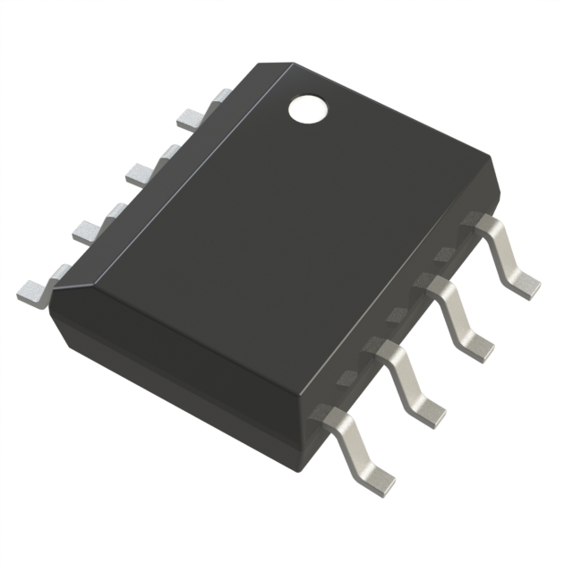
ISL6622CBZ
ObsoleteVR11.1 COMPATIBLE SYNCHRONOUS RECTIFIED BUCK MOSFET DRIVERS
Deep-Dive with AI
Search across all available documentation for this part.

ISL6622CBZ
ObsoleteVR11.1 COMPATIBLE SYNCHRONOUS RECTIFIED BUCK MOSFET DRIVERS
Deep-Dive with AI
Technical Specifications
Parameters and characteristics for this part
| Specification | ISL6622CBZ |
|---|---|
| Channel Type | Synchronous |
| Current - Peak Output (Source, Sink) [custom] | 1.25 A |
| Current - Peak Output (Source, Sink) [custom] | 2 A |
| Driven Configuration | Half-Bridge |
| Gate Type | N-Channel MOSFET |
| Input Type | Non-Inverting |
| Mounting Type | Surface Mount |
| Number of Drivers | 2 |
| Operating Temperature [Max] | 125 ¯C |
| Operating Temperature [Min] | 0 °C |
| Package / Case | 8-SOIC |
| Package / Case [x] | 0.154 in |
| Package / Case [y] | 3.9 mm |
| Rise / Fall Time (Typ) [custom] | 18 ns |
| Rise / Fall Time (Typ) [custom] | 26 ns |
| Supplier Device Package | 8-SOIC |
| Voltage - Supply [Max] | 13.2 V |
| Voltage - Supply [Min] | 6.8 V |
Pricing
Prices provided here are for design reference only. For realtime values and availability, please visit the distributors directly
| Distributor | Package | Quantity | $ | |
|---|---|---|---|---|
Description
General part information
ISL6622A Series
The ISL6622 is a high frequency MOSFET driver designed to drive upper and lower power N-Channel MOSFETs in a synchronous rectified buck converter topology. The advanced PWM protocol of ISL6622 is specifically designed to work with Intersil VR11. 1 controllers and combined with N-Channel MOSFETs, form a complete core-voltage regulator solution for advanced microprocessors. When ISL6622 detects a PSI protocol sent by an Intersil VR11. 1 controller, it activates Diode Emulation (DE) and Gate Voltage Optimization Technology (GVOT) operation; otherwise, it operates in normal Continuous Conduction Mode (CCM) PWM mode. In the 8 Ld SOIC package, the ISL6622 drives the upper and lower gates to VCC during normal PWM mode, while the lower gate drops down to a fixed 5. 75V (typically) during PSI mode. The 10 Ld DFN part offers more flexibility: the upper gate can be driven from 5V to 12V via the UVCC pin, while the lower gate has a resistor-selectable drive voltage of 5. 75V, 6. 75V, and 7. 75V (typically) during PSI mode. This provides the flexibility necessary to optimize applications involving trade-offs between gate charge and conduction losses. To further enhance light load efficiency, the ISL6622 enables diode emulation operation during PSI mode. This allows Discontinuous Conduction Mode (DCM) by detecting when the inductor current reaches zero and subsequently turning off the low side MOSFET to prevent it from sinking current. An advanced adaptive shoot-through protection is integrated to prevent both the upper and lower MOSFETs from conducting simultaneously and to minimize dead time. The ISL6622 has a 20kΩ integrated high-side gate-to-source resistor to prevent self turn-on due to high input bus dV/dt. This driver also has an overvoltage protection feature operational while VCC is below the POR threshold: the PHASE node is connected to the gate of the low side MOSFET (LGATE) via a 10kΩ resistor, limiting the output voltage of the converter close to the gate threshold of the low side MOSFET, dependent on the current being shunted, which provides some protection to the load should the upper MOSFET(s) become shorted.
Documents
Technical documentation and resources


