Deep-Dive with AI
Search across all available documentation for this part.

Deep-Dive with AI
Technical Specifications
Parameters and characteristics for this part
| Specification | SE555JGB |
|---|---|
| Current - Supply | 12 mA |
| Frequency [Max] | 100 kHz |
| Frequency [Min] | 1 mHz |
| Mounting Type | Through Hole |
| Operating Temperature [Max] | 125 °C |
| Operating Temperature [Min] | -55 °C |
| Package / Case | 7.62 mm |
| Package / Case | 0.3 in |
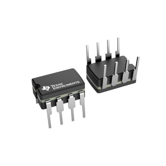
| Package / Case | 8-CDIP |
| Supplier Device Package | 8-CDIP |
| Type | 555 Type, Timer/Oscillator (Single) |
| Voltage - Supply [Max] | 18 V |
| Voltage - Supply [Min] | 4.5 V |
Pricing
Prices provided here are for design reference only. For realtime values and availability, please visit the distributors directly
| Distributor | Package | Quantity | $ | |
|---|---|---|---|---|
| Texas Instruments | TUBE | 1 | $ 31.01 | |
| 100 | $ 27.09 | |||
| 250 | $ 20.88 | |||
| 1000 | $ 18.68 | |||
Description
General part information
SE555M Series
The Nx555 and Sx555 devices are precision timing circuits capable of producing accurate time delays or oscillation. In time-delay or monostable operating modes, the timed interval is controlled by a single external resistor and capacitor network. In the astable mode of operation, the frequency and duty cycle are controlled independently with two external resistors and a single external capacitor.
Each timer has a trigger level equal to approximately one-third of the supply voltage and a threshold level equal to approximately two-thirds of the supply voltage. These levels can be altered by use of the control voltage pin (CONT). When the trigger input (TRIG) is less than the trigger level, the flip-flop is set and the output goes high. If TRIG is greater than the trigger level and the threshold input (THRES) is greater than the threshold level, the flip-flop is reset and the output is low. The reset input (RESET) overrides all other inputs and is used to initiate a new timing cycle. If RESET is low, the flip-flop is reset and the output is low. Whenever the output is low, a low-impedance path is provided between the discharge pin (DISCH) and the ground pin (GND). Tie all unused inputs to an appropriate logic level to prevent false triggering
The output circuit is capable of sinking or sourcing current up to 200mA. Operation is specified for supplies of 5V to 15V. With a 5V supply, output levels are compatible with TTL inputs.
Documents
Technical documentation and resources


