THS0842IPFB
ActiveDUAL-CHANNEL, 8-BIT, 40-MSPS ANALOG-TO-DIGITAL CONVERTER (ADC)
Deep-Dive with AI
Search across all available documentation for this part.

THS0842IPFB
ActiveDUAL-CHANNEL, 8-BIT, 40-MSPS ANALOG-TO-DIGITAL CONVERTER (ADC)
Deep-Dive with AI
Technical Specifications
Parameters and characteristics for this part
| Specification | THS0842IPFB |
|---|---|
| Architecture | Pipelined |
| Configuration | S/H-MUX-ADC |
| Data Interface | Parallel |
| Features | Simultaneous Sampling |
| Input Type | Single Ended, Differential |
| Mounting Type | Surface Mount |
| Number of A/D Converters | 1 |
| Number of Bits | 8 |
| Number of Inputs | 2 |
| Operating Temperature [Max] | 85 °C |
| Operating Temperature [Min] | -40 °C |
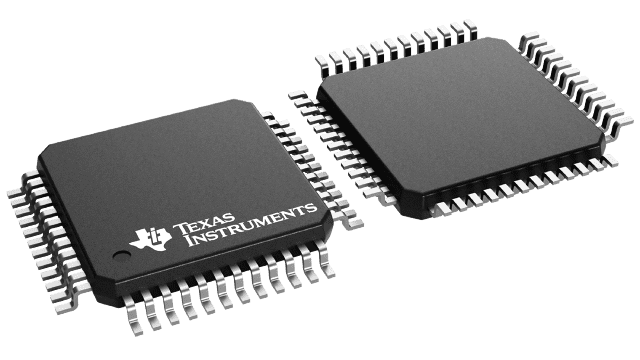
| Package / Case | 48-TQFP |
| Ratio - S/H:ADC | |
| Reference Type | External, Internal |
| Sampling Rate (Per Second) | 40M |
| Supplier Device Package | 48-TQFP (7x7) |
| Voltage - Supply, Analog [Max] | 3.6 V |
| Voltage - Supply, Analog [Min] | 3 V |
| Voltage - Supply, Digital [Max] | 3.6 V |
| Voltage - Supply, Digital [Min] | 3 V |
Pricing
Prices provided here are for design reference only. For realtime values and availability, please visit the distributors directly
| Distributor | Package | Quantity | $ | |
|---|---|---|---|---|
| Digikey | Tray | 250 | $ 14.44 | |
| Texas Instruments | JEDEC TRAY (10+1) | 1 | $ 17.61 | |
| 100 | $ 15.39 | |||
| 250 | $ 11.86 | |||
| 1000 | $ 10.61 | |||
Description
General part information
THS0842 Series
The THS0842 is a dual 8-bit 40 MSPS high-speed A/D converter. It alternately converts each analog input signal into 8-bit binary-coded digital words up to a maximum sampling rate of 40 MSPS with an 80 MHz clock. All digital inputs and outputs are 3.3 V TTL/CMOS-compatible.
Thanks to an innovative single-pipeline architecture implemented in a CMOS process and the 3.3 V supply, the device consumes very little power. In order to provide maximum flexibility, both bottom and top voltage references can be set from user supplied voltages. Alternately, if no external references are available, on-chip references can be used which are also made available externally. The full-scale range is 1 Vpp, depending on the analog supply voltage. If external references are available, the internal references can be powered down independently from the rest of the chip, resulting in an even greater power saving.
The device is specifically suited for the baseband sampling of wireless local loop (WLL) communication, cable modems, set top boxes (STBs), and test instruments.
Documents
Technical documentation and resources


