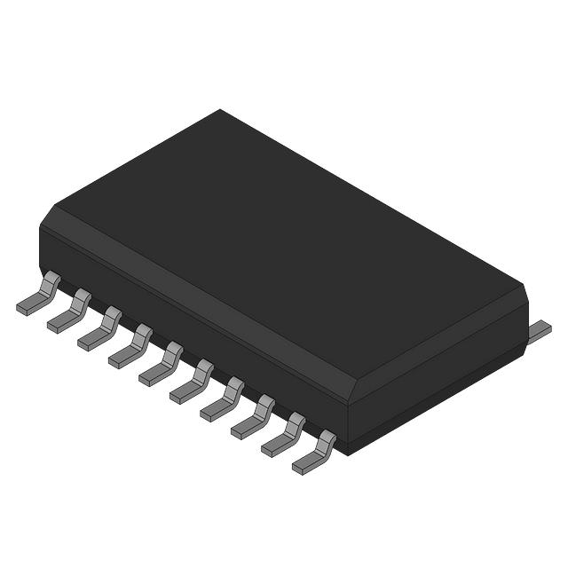
MM74HCT374SJX
ActiveFLIP FLOP D-TYPE BUS INTERFACE POS-EDGE 3-ST 1-ELEMENT 20-PIN SOP-II T/R
Deep-Dive with AI
Search across all available documentation for this part.

MM74HCT374SJX
ActiveFLIP FLOP D-TYPE BUS INTERFACE POS-EDGE 3-ST 1-ELEMENT 20-PIN SOP-II T/R
Deep-Dive with AI
Technical Specifications
Parameters and characteristics for this part
| Specification | MM74HCT374SJX |
|---|---|
| Clock Frequency | 30 MHz |
| Current - Output High, Low | 7.2 mA, 7.2 mA |
| Current - Quiescent (Iq) | 8 ÁA |
| Function | Standard |
| Input Capacitance | 10 pF |
| Max Propagation Delay @ V, Max CL | 46 ns |
| Mounting Type | Surface Mount |
| Number of Bits per Element | 8 |
| Number of Elements | 1 |
| Operating Temperature [Max] | 85 °C |
| Operating Temperature [Min] | -40 °C |
| Output Type | Tri-State, Non-Inverted |
| Package / Case | 20-SOIC |
| Package / Case | 0.209 " |
| Package / Case | 5.3 mm |
| Supplier Device Package | 20-SOP |
| Trigger Type | Positive Edge |
| Type | D-Type |
| Voltage - Supply [Max] | 5.5 V |
| Voltage - Supply [Min] | 4.5 V |
Pricing
Prices provided here are for design reference only. For realtime values and availability, please visit the distributors directly
| Distributor | Package | Quantity | $ | |
|---|---|---|---|---|
| Digikey | Bulk | 511 | $ 0.59 | |
Description
General part information
MC74HCT374A Series
The MM74HCT373 octal D-type latches and MM74HCT374 Octal D-type flip flops advanced silicon-gate CMOS technology, which provides the inherent benefits of low power consumption and wide power supply range, but are LS-TTL input and output characteristic & pin-out compatible. The 3-STATE outputs are capable of driving 15 LS-TTL loads. All inputs are protected from damage due to static discharge by internal diodes to VCCand ground. When the MM74HCT373 LATCH ENABLE input is HIGH, the Q outputs will follow the D inputs. When the LATCH ENABLE goes LOW, data at the D inputs will be retained at the outputs until LATCH ENABLE returns HIGH again. When a high logic level is applied to the OUTPUT CONTROL input, all outputs go to a high impedance state, regardless of what signals are present at the other inputs and the state of the storage elements. The MM74HCT374 are positive edge triggered flip-flops. Data at the D inputs, meeting the setup and hold time requirements, are transferred to the Q outputs on positive going transitions of the CLOCK (CK) input. When a high logic level is applied to the OUTPUT CONTROL (OC) input, all outputs go to a high impedance state, regardless of what signals are present at the other inputs and the state of the storage elements. MM74HCT devices are intended to interface between TTL and NMOS components and standard CMOS devices. These parts are also plug in replacements for LS-TTL devices and can be used to reduce power consumption in existing designs.
Documents
Technical documentation and resources
No documents available


