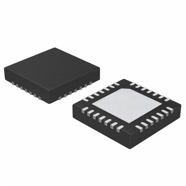
5T9306NLGI
ActiveCLOCK BUFFER, 1GHZ, -40 TO 85DEG C ROHS COMPLIANT: YES
Deep-Dive with AI
Search across all available documentation for this part.

5T9306NLGI
ActiveCLOCK BUFFER, 1GHZ, -40 TO 85DEG C ROHS COMPLIANT: YES
Deep-Dive with AI
Technical Specifications
Parameters and characteristics for this part
| Specification | 5T9306NLGI |
|---|---|
| Differential - Input:Output | True |
| Frequency - Max [Max] | 1 GHz |
| Input | eHSTL, HSTL, LVTTL, LVPECL, LVDS, CML |
| Mounting Type | Surface Mount |
| Number of Circuits | 1 |
| Operating Temperature [Max] | 85 °C |
| Operating Temperature [Min] | -40 C |
| Output | LVDS |
| Package / Case | 28-VQFN Exposed Pad |
| Ratio - Input:Output | 2:6 |
| Supplier Device Package | 28-VFQFPN (6x6) |
| Type | Fanout Buffer (Distribution), Multiplexer |
| Voltage - Supply [Max] | 2.7 V |
| Voltage - Supply [Min] | 2.3 V |
| Part | Mounting Type | Ratio - Input:Output | Number of Circuits | Package / Case | Voltage - Supply [Min] | Voltage - Supply [Max] | Differential - Input:Output | Output | Frequency - Max [Max] | Input | Type | Supplier Device Package | Operating Temperature [Max] | Operating Temperature [Min] |
|---|---|---|---|---|---|---|---|---|---|---|---|---|---|---|
Renesas Electronics Corporation | Surface Mount | 2:6 | 1 | 28-VQFN Exposed Pad | 2.3 V | 2.7 V | LVDS | 1 GHz | CML eHSTL HSTL LVDS LVPECL LVTTL | Fanout Buffer (Distribution) Multiplexer | 28-VFQFPN (6x6) | 85 °C | -40 C | |
Renesas Electronics Corporation | Surface Mount | 2:6 | 1 | 28-VQFN Exposed Pad | 2.3 V | 2.7 V | LVDS | 1 GHz | CML eHSTL HSTL LVDS LVPECL LVTTL | Fanout Buffer (Distribution) Multiplexer | 28-VFQFPN (6x6) | 85 °C | -40 C |
Pricing
Prices provided here are for design reference only. For realtime values and availability, please visit the distributors directly
Description
General part information
5T9306 Series
The 5T9306 2.5V differential clock buffer is a user-selectable differential input to six LVDS outputs. The fanout from a differential input to six LVDS outputs reduces loading on the preceding driver and provides an efficient clock distribution network. The 5T9306 can act as a translator from a differential HSTL, eHSTL, LVEPECL (2.5V), LVPECL (3.3V), CML, or LVDS input to LVDS outputs. A single-ended 3.3V / 2.5V LVTTL input can also be used to translate to LVDS outputs. The redundant input capability allows for an asynchronous change-over from a primary clock source to a secondary clock source. Selectable reference inputs are controlled by SEL. The 5T9306 outputs can be asynchronously enabled/disabled. When disabled, the outputs will drive to the value selected by the GL pin. Multiple power and grounds reduce noise.
Documents
Technical documentation and resources


