Deep-Dive with AI
Search across all available documentation for this part.

Deep-Dive with AI
Technical Specifications
Parameters and characteristics for this part
| Specification | TLC6C598QDRQ1 |
|---|---|
| Current - Output / Channel | 50 mA |
| Grade | Automotive |
| Internal Switch(s) | True |
| Mounting Type | Surface Mount |
| Number of Outputs | 8 |
| Operating Temperature [Max] | 125 °C |
| Operating Temperature [Min] | -40 °C |
| Package / Case | 16-SOIC |
| Package / Case [x] | 0.154 in |
| Package / Case [y] | 3.9 mm |
| Qualification | AEC-Q100 |
| Supplier Device Package | 16-SOIC |
| Topology | Shift Register |
| Type | Power Switch |
| Voltage - Output | 40 V |
| Voltage - Supply (Max) | 5.5 V |
| Voltage - Supply (Min) [Min] | 3 V |
Pricing
Prices provided here are for design reference only. For realtime values and availability, please visit the distributors directly
| Distributor | Package | Quantity | $ | |
|---|---|---|---|---|
Description
General part information
TLC6C598-Q1 Series
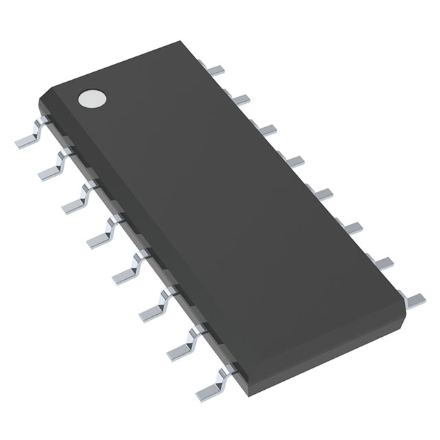
The TLC6C598-Q1 is a monolithic, medium-voltage, low-current power 8-bit shift register designed for use in systems that require relatively moderate load power, such as LEDs.
This device contains an 8-bit serial-in, parallel-out shift register that feeds an 8-bit D-type storage register. Data transfers through both the shift and storage registers on the rising edge of the shift-register clock (SRCK) and the register clock (RCK), respectively. The storage register transfers data to the output buffer when shift register clear (CLR) is high. A low onCLRclears all registers in the device. Holding the output enable (G) high, holds all data in the output buffers low, and all drain outputs are off. HoldingGlow makes data from the storage register transparent to the output buffers. When data in the output buffers is low, the DMOS transistor outputs are off. When data is high, the DMOS transistor outputs have sink-current capability. The serial output (SER OUT) clocks out of the device on the falling edge of SRCK to provide additional hold time for cascaded applications. This provides improved performance for applications where clock signals may be skewed, devices are not located near one another, or the system must tolerate electromagnetic interference. The device contains built-in thermal shutdown protection.
Outputs are low-side, open-drain DMOS transistors with output ratings of 40 V and 50 mA continuous sink-current capabilities when Vcc = 5 V. The current limit decreases as the junction temperature increases for additional device protection. The device also provides up to 2000 V of ESD protection when tested using the human-body model and 200 V when using the machine model.
Documents
Technical documentation and resources
No documents available


