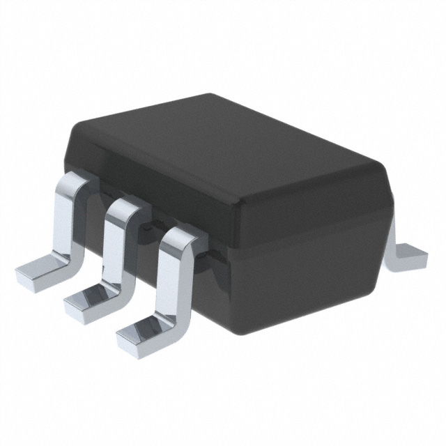
ADS7887SDCKR
Active2.35V-5.25V, 10 BIT, 1.25MSPS, SERIAL ADC
Deep-Dive with AI
Search across all available documentation for this part.

ADS7887SDCKR
Active2.35V-5.25V, 10 BIT, 1.25MSPS, SERIAL ADC
Deep-Dive with AI
Technical Specifications
Parameters and characteristics for this part
| Specification | ADS7887SDCKR |
|---|---|
| Architecture | SAR |
| Configuration | S/H-ADC |
| Data Interface | SPI |
| Input Type | Single Ended |
| Mounting Type | Surface Mount |
| Number of A/D Converters | 1 |
| Number of Bits [custom] | 10 |
| Number of Inputs | 1 |
| Operating Temperature [Max] | 125 °C |
| Operating Temperature [Min] | -40 °C |
| Package / Case | 6-TSSOP, SC-88, SOT-363 |
| Ratio - S/H:ADC | 1:1 |
| Reference Type | Supply |
| Sampling Rate (Per Second) | 1.25 M |
| Supplier Device Package | SC-70-6 |
| Voltage - Supply, Analog [Max] | 5.25 V |
| Voltage - Supply, Analog [Min] | 2.35 V |
| Voltage - Supply, Digital [Max] | 5.25 V |
| Voltage - Supply, Digital [Min] | 2.35 V |
Pricing
Prices provided here are for design reference only. For realtime values and availability, please visit the distributors directly
| Distributor | Package | Quantity | $ | |
|---|---|---|---|---|
| Digikey | Cut Tape (CT) | 1 | $ 3.68 | |
| 10 | $ 3.31 | |||
| 25 | $ 3.12 | |||
| 100 | $ 2.71 | |||
| 250 | $ 2.57 | |||
| 500 | $ 2.31 | |||
| 1000 | $ 1.94 | |||
| Digi-Reel® | 1 | $ 3.68 | ||
| 10 | $ 3.31 | |||
| 25 | $ 3.12 | |||
| 100 | $ 2.71 | |||
| 250 | $ 2.57 | |||
| 500 | $ 2.31 | |||
| 1000 | $ 1.94 | |||
| Tape & Reel (TR) | 3000 | $ 1.85 | ||
| Texas Instruments | LARGE T&R | 1 | $ 2.78 | |
| 100 | $ 2.43 | |||
| 250 | $ 1.71 | |||
| 1000 | $ 1.38 | |||
Description
General part information
ADS7887 Series
The ADS7887 device is a 10-bit, 1.25-MSPS, analog-to-digital converter (ADC), and the ADS7888 device is a 8-bit, 1.25-MSPS ADC. These devices include a capacitor-based SAR A/D converter with inherent sample and hold. The serial interface in each device is controlled by theCSand SCLK signals for glueless connections with microprocessors and DSPs. The input signal is sampled with the falling edge ofCS, and SCLK is used for conversion and serial data output.
The devices operate from a wide supply range from 2.35 V to 5.25 V. The low power consumption of the devices make them suitable for battery-powered applications. The devices also include a power-saving, power-down feature for when the devices are operated at lower conversion speeds.
The high level of the digital input to the device is not limited to device VDD. This means the digital input can go as high as 5.25 V when device supply is 2.35 V. This feature is useful when digital signals are coming from other circuit with different supply levels. Also this relaxes restriction on power-up sequencing.
Documents
Technical documentation and resources


