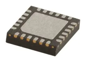
BD8P250MUF-CE2
ActiveQUICK BUCK BOOSTER™, NANO PULSE CONTROL™, 2.7 V TO 36 V INPUT, 2 A SINGLE BUCK DC/DC CONVERTER WITH BOOST FUNCTION FOR AUTOMOTIVE
Deep-Dive with AI
Search across all available documentation for this part.

BD8P250MUF-CE2
ActiveQUICK BUCK BOOSTER™, NANO PULSE CONTROL™, 2.7 V TO 36 V INPUT, 2 A SINGLE BUCK DC/DC CONVERTER WITH BOOST FUNCTION FOR AUTOMOTIVE
Deep-Dive with AI
Technical Specifications
Parameters and characteristics for this part
| Specification | BD8P250MUF-CE2 |
|---|---|
| Current - Output | 2 A |
| Frequency - Switching | 2.2 MHz |
| Function | Step-Down, Step-Up/Step-Down |
| Mounting Type | Surface Mount |
| Number of Outputs | 1 |
| Operating Temperature [Max] | 125 °C |
| Operating Temperature [Min] | -40 °C |
| Output Configuration | Positive |
| Package / Case | 24-VFQFN Exposed Pad |
| Supplier Device Package | VQFN24FV4040 |
| Synchronous Rectifier | True |
| Topology | Buck-Boost, Buck |
| Voltage - Input (Max) [Max] | 36 V |
| Voltage - Input (Min) | 3.5 V, 2.7 V |
| Voltage - Output (Min/Fixed) | 5 V |
Pricing
Prices provided here are for design reference only. For realtime values and availability, please visit the distributors directly
| Distributor | Package | Quantity | $ | |
|---|---|---|---|---|
| Digikey | Cut Tape (CT) | 1 | $ 4.19 | |
| 10 | $ 3.17 | |||
| 25 | $ 2.92 | |||
| 100 | $ 2.64 | |||
| 250 | $ 2.50 | |||
| 500 | $ 2.42 | |||
| 1000 | $ 2.36 | |||
| Digi-Reel® | 1 | $ 4.19 | ||
| 10 | $ 3.17 | |||
| 25 | $ 2.92 | |||
| 100 | $ 2.64 | |||
| 250 | $ 2.50 | |||
| 500 | $ 2.42 | |||
| 1000 | $ 2.36 | |||
| N/A | 9053 | $ 4.19 | ||
| Tape & Reel (TR) | 2500 | $ 2.29 | ||
Description
General part information
BD8P250MUF-C Series
The BD8P250MUF-C is a synchronous rectification buck DC/DC converter with boost control function that utilizes ROHM’s Quick Buck Booster™ technology to achieve improved response even when switching buck-boost operation, reducing the number of output capacitors by half over conventional solutions.This technology supports a common design for both boost and buck-boost applications. Use the BD8P250MUF-C as a single-chip buck DC/DC converter for cold cranking or other instances where a drop in the output voltage is acceptable during the input voltage drop. Or, if the output voltage must be maintained, it can be utilized in a buck-boost DC/DC configuration by addinga dedicated boost-FET.Additional features include a spread spectrum function that minimizes EMI, making it possible to easily clear the CISPR 25 Class 5 standard for noise in automotive electrical components. And leveraging original Nano Pulse technology reduces no-load current consumption to an unprecedented 8μA at 5V output from a 12V battery. This translates to 73% greater efficiency in buck and buck-boost operation at 0.1mA output load current over competitor products.
Documents
Technical documentation and resources


