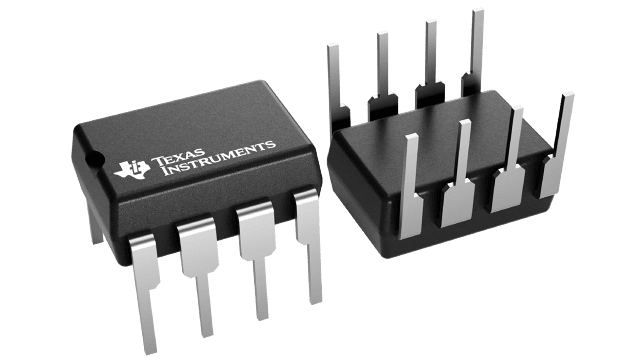
TL7660IP
ActiveCHARGE PUMP INV/STPUP/STPDN -1.5V TO -10V 100MA 8-PIN PDIP TUBE
Deep-Dive with AI
Search across all available documentation for this part.

TL7660IP
ActiveCHARGE PUMP INV/STPUP/STPDN -1.5V TO -10V 100MA 8-PIN PDIP TUBE
Deep-Dive with AI
Technical Specifications
Parameters and characteristics for this part
| Specification | TL7660IP |
|---|---|
| Frequency - Switching | 10 kHz |
| Function | Ratiometric |
| Mounting Type | Through Hole |
| Number of Outputs | 1 |
| Operating Temperature [Max] | 125 °C |
| Operating Temperature [Min] | -40 °C |
| Output Configuration | Positive or Negative |
| Output Type | 1.81 mOhm |
| Package / Case | 0.3 in |
| Package / Case | 8-DIP |
| Package / Case | 7.62 mm |
| Supplier Device Package | 8-PDIP |
| Synchronous Rectifier | False |
| Voltage - Input (Max) [Max] | 10 V |
| Voltage - Input (Min) [Min] | 1.5 V |
| Voltage - Output (Min/Fixed) [Max] | 2Vin |
| Voltage - Output (Min/Fixed) [Min] | -Vin |
Pricing
Prices provided here are for design reference only. For realtime values and availability, please visit the distributors directly
| Distributor | Package | Quantity | $ | |
|---|---|---|---|---|
| Arrow | N/A | 50 | $ 0.73 | |
| Digikey | Tube | 1 | $ 1.88 | |
| 10 | $ 1.69 | |||
| 50 | $ 1.59 | |||
| 100 | $ 1.36 | |||
| 250 | $ 1.27 | |||
| 500 | $ 1.12 | |||
| 1000 | $ 0.92 | |||
| 2500 | $ 0.86 | |||
| 5000 | $ 0.83 | |||
| Texas Instruments | TUBE | 1 | $ 1.56 | |
| 100 | $ 1.20 | |||
| 250 | $ 0.88 | |||
| 1000 | $ 0.63 | |||
Description
General part information
TL7660 Series
The TL7660 is a CMOS switched-capacitor voltage converter that perform supply-voltage conversions from positive to negative. With only two noncritical external capacitors needed for the charge pump and charge reservoir functions, an input voltage within the range from 1.5 V to 10 V is converted to a complementary negative output voltage of -1.5 V to -10 V. The device can also be connected as a voltage doubler to generate output voltages up to 18.6 V with a 10-V input.
The basic building blocks of the IC include a linear regulator, an RC oscillator, a voltage-level translator, and four power MOS switches. To ensure latch-up-free operation, the circuitry automatically senses the most negative voltage in the device and ensures that the N-channel switch source-substrate junctions are not forward biased. The oscillator frequency runs at a nominal 10 kHz (for VCC= 5 V), but that frequency can be decreased by adding an external capacitor to the oscillator (OSC) terminal or increased by overdriving OSC with an external clock.
For low-voltage operation (VIN< 3.5 V), LV should be tied to GND to bypass the internal series regulator. Above 3.5 V, LV should be left floating to prevent device latchup.
Documents
Technical documentation and resources


