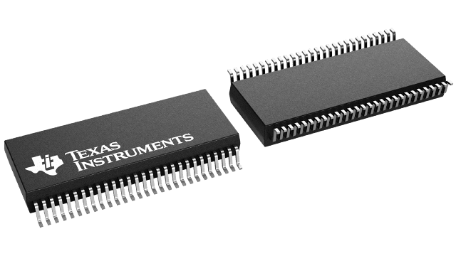
SN74ABTH162260DL
Active12-BIT TO 24-BIT MULTIPLEXED D-TYPE LATCHES WITH SERIES-DAMPING RESISTORS AND 3-STATE OUTPUTS
Deep-Dive with AI
Search across all available documentation for this part.

SN74ABTH162260DL
Active12-BIT TO 24-BIT MULTIPLEXED D-TYPE LATCHES WITH SERIES-DAMPING RESISTORS AND 3-STATE OUTPUTS
Technical Specifications
Parameters and characteristics for this part
| Specification | SN74ABTH162260DL |
|---|---|
| Circuit | 12:24 |
| Current - Output High, Low [custom] | 64 mA |
| Current - Output High, Low [custom] | 32 mA |
| Delay Time - Propagation | 3.6 ns |
| Independent Circuits | 1 |
| Logic Type | D-Type Transparent Latch |
| Mounting Type | Surface Mount |
| Operating Temperature [Max] | 85 °C |
| Operating Temperature [Min] | -40 °C |
| Output Type | Tri-State |
| Package / Case | 0.295 in |
| Package / Case | 56-BSSOP |
| Package / Case | 7.5 mm |
| Supplier Device Package | 56-SSOP |
| Voltage - Supply [Max] | 5.5 V |
| Voltage - Supply [Min] | 4.5 V |
Pricing
Prices provided here are for design reference only. For realtime values and availability, please visit the distributors directly
| Distributor | Package | Quantity | $ | |
|---|---|---|---|---|
| Digikey | Tube | 320 | $ 3.05 | |
| Texas Instruments | TUBE | 1 | $ 3.30 | |
| 100 | $ 2.89 | |||
| 250 | $ 2.03 | |||
| 1000 | $ 1.63 | |||
Description
General part information
SN74ABTH162260 Series
The 'ABTH162260 are 12-bit to 24-bit multiplexed D-type latches used in applications where two separate data paths must be multiplexed onto, or demultiplexed from, a single data path. Typical applications include multiplexing and/or demultiplexing of address and data information in microprocessor or bus-interface applications. These devices are also useful in memory-interleaving applications.
Three 12-bit I/O ports (A1-A12, 1B1-1B12, and 2B1-2B12) are available for address and/or data transfer. The output-enable (OE1B\, OE2B\, and OEA\) inputs control the bus-transceiver functions. The OE1B\ and OE2B\ control signals also allow bank control in the A-to-B direction.
Address and/or data information can be stored using the internal storage latches. The latch-enable (LE1B, LE2B, LEA1B, and LEA2B) inputs are used to control data storage. When the latch-enable input is high, the latch is transparent. When the latch-enable input goes low, the data present at the inputs is latched and remains latched until the latch-enable input is returned high.
Documents
Technical documentation and resources


