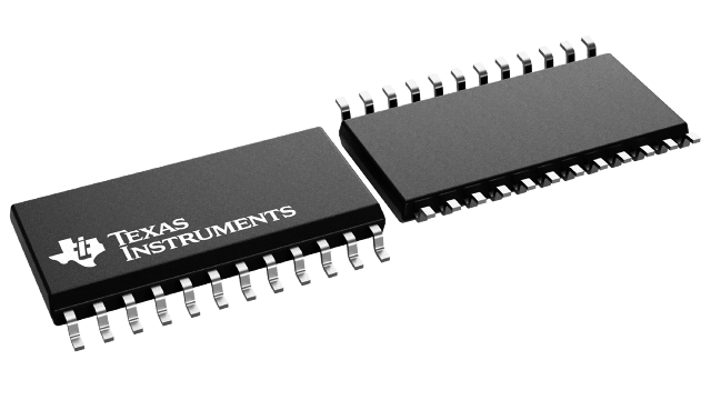
SN74ACT2228DW
Active256 X 1 X 2 DUAL INDEPENDENT SYNCHRONOUS FIFO MEMORIES
Deep-Dive with AI
Search across all available documentation for this part.

SN74ACT2228DW
Active256 X 1 X 2 DUAL INDEPENDENT SYNCHRONOUS FIFO MEMORIES
Deep-Dive with AI
Technical Specifications
Parameters and characteristics for this part
| Specification | SN74ACT2228DW |
|---|---|
| Access Time | 20 ns |
| Bus Directional | Uni-Directional |
| Current - Supply (Max) [Max] | 400 µA |
| Data Rate | 22 MHz |
| Function | Synchronous |
| FWFT Support | False |
| Memory Size | 512 |
| Mounting Type | Surface Mount |
| Operating Temperature [Max] | 85 °C |
| Operating Temperature [Min] | -40 °C |
| Package / Case | 24-SOIC |
| Package / Case [custom] | 7.5 mm |
| Package / Case [custom] | 0.295 in |
| Programmable Flags Support | False |
| Retransmit Capability | False |
| Supplier Device Package | 24-SOIC |
| Voltage - Supply [Max] | 5.5 V |
| Voltage - Supply [Min] | 4.5 V |
Pricing
Prices provided here are for design reference only. For realtime values and availability, please visit the distributors directly
| Distributor | Package | Quantity | $ | |
|---|---|---|---|---|
| Digikey | Tube | 25 | $ 7.89 | |
| 50 | $ 7.86 | |||
| 125 | $ 7.05 | |||
| 250 | $ 6.84 | |||
| 625 | $ 6.50 | |||
| 1250 | $ 6.28 | |||
| Texas Instruments | TUBE | 1 | $ 9.23 | |
| 100 | $ 7.52 | |||
| 250 | $ 5.91 | |||
| 1000 | $ 5.01 | |||
Description
General part information
SN74ACT2228 Series
The SN74ACT2226 and SN74ACT2228 are dual FIFOs suited for a wide range of serial-data buffering applications, including elastic stores for frequencies up to T2 telecommunication rates. Each FIFO on the chip is arranged as 64 × 1 (SN74ACT2226) or 256 × 1 (SN74ACT2228) and has control signals and status flags for independent operation. Output flags for each FIFO include input ready (1IR or 2IR), output ready (1OR or 2OR), half full (1HF or 2HF), and almost full/almost empty (1AF/AE or 2AF/AE).
Serial data is written into a FIFO on the low-to-high transition of the write-clock (1WRTCLK or 2WRTCLK) input when the write-enable (1WRTEN or 2WRTEN) input and input-ready flag (1IR or 2IR) output are both high. Serial data is read from a FIFO on the low-to-high transition of the read-clock (1RDCLK or 2RDCLK) input when the read-enable (1RDEN or 2RDEN) input and output-ready flag (1OR or 2OR) output are both high. The read and write clocks of a FIFO can be asynchronous to one another.
Each input-ready flag (1IR or 2IR) is synchronized by two flip-flop stages to its write clock (1WRTCLK or 2WRTCLK), and each output-ready flag (1OR or 2OR) is synchronized by three flip-flop stages to its read clock (1RDCLK or 2RDCLK). This multistage synchronization ensures reliable flag-output states when data is written and read asynchronously.
Documents
Technical documentation and resources


