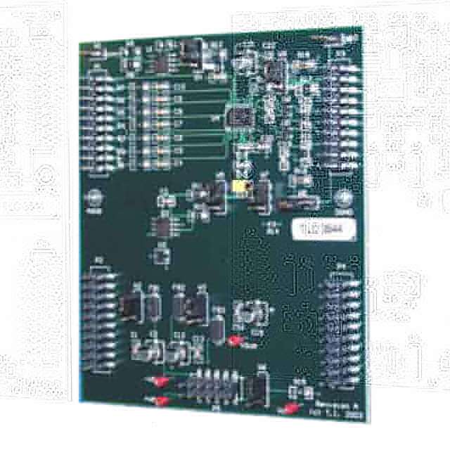
TLC3544EVM
ObsoleteEVALUATION MODULE FOR TLC3544
Deep-Dive with AI
Search across all available documentation for this part.

TLC3544EVM
ObsoleteEVALUATION MODULE FOR TLC3544
Deep-Dive with AI
Technical Specifications
Parameters and characteristics for this part
| Specification | TLC3544EVM |
|---|---|
| Data Interface | Serial |
| Input Range [Max] | 5 V |
| Input Range [Min] | 0 V |
| Number of A/D Converters | 1 |
| Number of Bits | 14 |
| Sampling Rate (Per Second) | 200k |
| Supplied Contents | Board(s) |
| Utilized IC / Part | TLC3544 |
Pricing
Prices provided here are for design reference only. For realtime values and availability, please visit the distributors directly
| Distributor | Package | Quantity | $ | |
|---|---|---|---|---|
Description
General part information
TLC3545 Series
The TLC3541 and TLC3545 are a family of high performance, 14-bit, low power, miniature CMOS analog-to-digital converters (ADCs). These devices operate from a single 5-V supply. Devices are available with single, dual, or single pseudo-differential inputs. All of these devices have a chip select (CS)\, serial clock (SCLK), and serial data output (SDO) that provides a direct 3-wire interface to the serial port of most popular host microprocessors (SPI interface). When interfaced with a DSP, a frame sync signal (FS) is used to indicate the start of a serial data frame on either pin 1 (CS)\ or pin 7 (FS) for the TLC3541. The TLC3545 ADC connects to the DSP via pin 1 only (CS)\.
The TLC3541 and TLC3545 are designed to operate with low power consumption. The power saving feature is further enhanced with an auto-power down mode. This product family features a high-speed serial link to modern host processors with an external SCLK up to 15 MHz. Both families use a built-in oscillator as the conversion clock, providing a 2.67 us maximum conversion time.
The TLC3541 and TLC3545 are a family of high performance, 14-bit, low power, miniature CMOS analog-to-digital converters (ADCs). These devices operate from a single 5-V supply. Devices are available with single, dual, or single pseudo-differential inputs. All of these devices have a chip select (CS)\, serial clock (SCLK), and serial data output (SDO) that provides a direct 3-wire interface to the serial port of most popular host microprocessors (SPI interface). When interfaced with a DSP, a frame sync signal (FS) is used to indicate the start of a serial data frame on either pin 1 (CS)\ or pin 7 (FS) for the TLC3541. The TLC3545 ADC connects to the DSP via pin 1 only (CS)\.
Documents
Technical documentation and resources


