Deep-Dive with AI
Search across all available documentation for this part.

Deep-Dive with AI
Technical Specifications
Parameters and characteristics for this part
| Specification | SN75C1154DW |
|---|---|
| Duplex | Full |
| Mounting Type | Surface Mount |
| Number of Drivers/Receivers [custom] | 4 |
| Number of Drivers/Receivers [custom] | 4 |
| Operating Temperature [Max] | 70 °C |
| Operating Temperature [Min] | 0 °C |
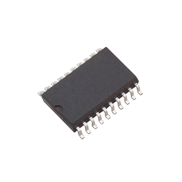
| Package / Case | 20-SOIC |
| Package / Case [y] | 0.295 in |
| Package / Case [y] | 7.5 mm |
| Protocol | RS232 |
| Receiver Hysteresis | 1 V |
| Supplier Device Package | 20-SOIC |
| Type | Transceiver |
| Voltage - Supply [Max] | 15 V |
| Voltage - Supply [Min] | 4.5 V |
Pricing
Prices provided here are for design reference only. For realtime values and availability, please visit the distributors directly
| Distributor | Package | Quantity | $ | |
|---|---|---|---|---|
| Digikey | Tube | 475 | $ 1.81 | |
| Texas Instruments | TUBE | 1 | $ 2.54 | |
| 100 | $ 2.22 | |||
| 250 | $ 1.56 | |||
| 1000 | $ 1.26 | |||
Description
General part information
SN75C1154 Series
The SN65C1164 and SN75C1154 are low-power BiMOS devices containing four independent drivers and receivers that are used to interface data terminal equipment (DTE) with data circuit-terminating equipment (DCE). These devices are designed to conform to TIA/EIA-232-F. The drivers and receivers of the SN65C1154 and SN75C1154 are similar to those of the SN75C188 quadruple driver and SN75C189A quadruple receiver, respectively. The drivers have a controlled output slew rate that is limited to a maximum of 30 V/µs and the receivers have filters that reject input noise pulses of shorter than 1 µs. Both these features eliminate the need for external components.
The SN65C1154 and SN75C1154 have been designed using low-power techniques in a BiMOS technology. In most applications, the receivers contained in these devices interface to single inputs of peripheral devices such as ACEs, UARTs, or microprocessors. By using sampling, such peripheral devices usually are insensitive to the transition times of the input signals. If this is not the case, or for other uses, it is recommended that the SN65C1154 and SN75C1154 receiver outputs be buffered by single Schmitt input gates or single gates of the HCMOS, ALS, or 74F logic families.
The SN65C1164 and SN75C1154 are low-power BiMOS devices containing four independent drivers and receivers that are used to interface data terminal equipment (DTE) with data circuit-terminating equipment (DCE). These devices are designed to conform to TIA/EIA-232-F. The drivers and receivers of the SN65C1154 and SN75C1154 are similar to those of the SN75C188 quadruple driver and SN75C189A quadruple receiver, respectively. The drivers have a controlled output slew rate that is limited to a maximum of 30 V/µs and the receivers have filters that reject input noise pulses of shorter than 1 µs. Both these features eliminate the need for external components.
Documents
Technical documentation and resources


