Zenode.ai Logo
Beta

Technical Specifications

Parameters and characteristics for this part

SpecificationRCJ160N20TL
Current - Continuous Drain (Id) @ 25°C16 A
Drain to Source Voltage (Vdss)200 V
Drive Voltage (Max Rds On, Min Rds On)10 V
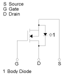
FET TypeN-Channel
Gate Charge (Qg) (Max) @ Vgs26 nC
Input Capacitance (Ciss) (Max) @ Vds1370 pF
Mounting TypeSurface Mount
Operating Temperature150 °C
Package / CaseD2PAK (2 Leads + Tab), TO-263-3, TO-263AB
Power Dissipation (Max)1.56 W, 40 W
Rds On (Max) @ Id, Vgs180 mOhm
Supplier Device PackageLPTS
TechnologyMOSFET (Metal Oxide)
Vgs (Max)30 V
Vgs(th) (Max) @ Id5.25 V

Pricing

Prices provided here are for design reference only. For realtime values and availability, please visit the distributors directly

DistributorPackageQuantity$
DigikeyN/A 1000$ 1.77

Description

General part information

RCJ160N20 Series

Power MOSFETs are made as low ON-resistance devices by the micro-processing technologies useful for wide range of applications. Broad lineup covering compact types, high-power types and complex types to meet various needs in the market.

Documents

Technical documentation and resources

Method for Calculating Junction Temperature from Transient Thermal Resistance Data

Thermal Design

Overview of ROHM's Simulation Models(for ICs and Discrete Semiconductors)

Technical Article

Basics of Thermal Resistance and Heat Dissipation

Thermal Design

About Export Regulations

Export Information

Method for Monitoring Switching Waveform

Schematic Design & Verification

Notes for Temperature Measurement Using Thermocouples

Thermal Design

How to Use LTspice® Models: Tips for Improving Convergence

Schematic Design & Verification

Judgment Criteria of Thermal Evaluation

Thermal Design

Taping Information

Package Information

MOSFET Gate Resistor Setting for Motor Driving

Technical Article

PCB Layout Thermal Design Guide

Thermal Design

List of Transistor Package Thermal Resistance

Thermal Design

Inner Structure

Package Information

Notes for Temperature Measurement Using Forward Voltage of PN Junction

Thermal Design

Report of SVHC under REACH Regulation

Environmental Data

θ<sub>JC</sub> and Ψ<sub>JT</sub>

Thermal Design

Condition of Soldering / Land Pattern Reference

Package Information

Reliability Test Result

Manufacturing Data

Two-Resistor Model for Thermal Simulation

Thermal Design

Precautions When Measuring the Rear of the Package with a Thermocouple

Thermal Design

What Is Thermal Design

Thermal Design

Importance of Probe Calibration When Measuring Power: Deskew

Schematic Design & Verification

Impedance Characteristics of Bypass Capacitor

Schematic Design & Verification

About Flammability of Materials

Environmental Data

Part Explanation

Application Note

Types and Features of Transistors

Application Note

Explanation for Marking

Package Information

θ<sub>JA</sub> and Ψ<sub>JT</sub>

Thermal Design

Temperature derating method for Safe Operating Area (SOA)

Schematic Design & Verification

Compliance of the RoHS directive

Environmental Data

Moisture Sensitivity Level - Transistors

Package Information

Measurement Method and Usage of Thermal Resistance RthJC

Thermal Design

ESD Data

Characteristics Data

Calculation of Power Dissipation in Switching Circuit

Schematic Design & Verification

Notes for Calculating Power Consumption:Static Operation

Thermal Design

How to Use LTspice&reg; Models

Schematic Design & Verification

Package Dimensions

Package Information

RCJ160N20 Data Sheet

Data Sheet

How to Use the Thermal Resistance and Thermal Characteristics Parameters

Thermal Design

What is a Thermal Model? (Transistor)

Thermal Design

Anti-Whisker formation - Transistors

Package Information

How to Create Symbols for PSpice Models

Models

Power Eco Family: Overview of ROHM's Power Semiconductor Lineup

White Paper

MOSFET Gate Drive Current Setting for Motor Driving

Technical Article