Deep-Dive with AI
Search across all available documentation for this part.

Deep-Dive with AI
Technical Specifications
Parameters and characteristics for this part
| Specification | SN74GTLP817DGVR |
|---|---|
| Channel Type | Bidirectional |
| Channels per Circuit | 6, 2 |
| Input Signal | GTLP |
| Mounting Type | Surface Mount |
| Number of Circuits | 2 |
| Operating Temperature [Max] | 85 °C |
| Operating Temperature [Min] | -40 °C |
| Output Signal | LVTTL |
| Output Type | Tri-State, Inverted |
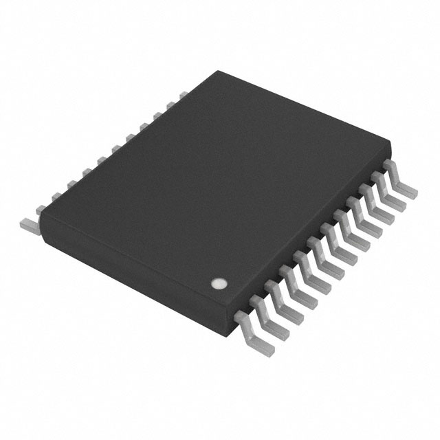
| Package / Case | 24-TFSOP |
| Package / Case [y] | 4.4 mm |
| Package / Case [y] | 0.173 in |
| Supplier Device Package | 24-TVSOP |
| Translator Type | Mixed Signal |
Pricing
Prices provided here are for design reference only. For realtime values and availability, please visit the distributors directly
| Distributor | Package | Quantity | $ | |
|---|---|---|---|---|
Description
General part information
SN74GTLP817 Series
The SN74GTLP817 is a medium-drive fanout driver that provides LVTTL-to-GTLP and GTLP-to-LVTTL signal-level translation. The device provides a high-speed interface between cards operating at LVTTL logic levels and a backplane operating at GTLP signal levels. High-speed (about three times faster than standard TTL or LVTTL) backplane operation is a direct result of GTLP reduced output swing (<1 V), reduced input threshold levels, improved differential input, and OEC™ circuitry. The improved GTLP OEC circuitry minimizes bus settling time and has been designed and tested using several backplane models. The medium drive allows incident-wave switching in heavily loaded backplanes with equivalent load impedance down to 19. BO1 and BO2 can be tied together to drive an equivalent load impedance down to 11.
GTLP is the Texas Instruments (TI™) derivative of the Gunning Transceiver Logic (GTL) JEDEC standard JESD 8-3. The ac specification of the SN74GTLP817 is given only at the preferred higher noise-margin GTLP, but the user has the flexibility of using this device at either GTL (VTT= 1.2 V and VREF= 0.8 V) or GTLP (VTT= 1.5 V and VREF= 1 V) signal levels.
Normally, the B port operates at GTLP signal levels. The A-port and control inputs operate at LVTTL logic levels but are 5-V tolerant and are compatible with TTL and 5-V CMOS inputs. VREFis the B-port differential input reference voltage.
Documents
Technical documentation and resources


