Deep-Dive with AI
Search across all available documentation for this part.

Deep-Dive with AI
Technical Specifications
Parameters and characteristics for this part
| Specification | NC7SVL08L6X |
|---|---|
| Current - Output High, Low | 24 mA |
| Current - Quiescent (Max) [Max] | 900 nA |
| Input Logic Level - High [Max] | 1.5 V |
| Input Logic Level - High [Min] | 0.9 V |
| Input Logic Level - Low [Max] | 0.8 V |
| Input Logic Level - Low [Min] | 0.7 V |
| Logic Type | AND Gate |
| Max Propagation Delay @ V, Max CL | 3.5 ns |
| Mounting Type | Surface Mount |
| Number of Circuits | 1 |
| Number of Inputs | 2 |
| Operating Temperature [Max] | 85 °C |
| Operating Temperature [Min] | -40 °C |
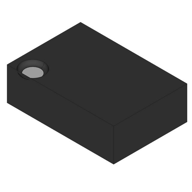
| Package / Case | 6-UFDFN |
| Supplier Device Package | 6-MicroPak |
| Voltage - Supply [Max] | 3.6 V |
| Voltage - Supply [Min] | 0.9 V |
Pricing
Prices provided here are for design reference only. For realtime values and availability, please visit the distributors directly
| Distributor | Package | Quantity | $ | |
|---|---|---|---|---|
| Digikey | Bulk | 1906 | $ 0.16 | |
Description
General part information
NC7SVL08 Series
The NC7SVL08 is a single two-input AND gate with a low-ICCTinput design from ON Semiconductor’s Ultra-Low Power (ULP-A) series of TinyLogic®. The NC7SVL08 features very low quiescent current, even when the input voltage is lower than the VCC supply. This feature services mobile handset applications very well, allowing for direct interface with baseband processor general-purpose I/Os. Since mobile devices rely on a battery supply, the NC7SVL08 facilitates lower power consumption in mixed-voltage rail environments.This product is designed on an advanced CMOS technology for a wide low-voltage operating range (0.9V to 3.6V VCC), high drive needs (up to 24mA), and speed (maximum propagation delay of 3.5ns, VCC=3.3V). It achieves this performance while maintaining low CMOS power dissipation.
Documents
Technical documentation and resources


