9214DGLF
ObsoleteIC CLOCK GEN RAMBUS XDR 28-TSSOP
Deep-Dive with AI
Search across all available documentation for this part.

9214DGLF
ObsoleteIC CLOCK GEN RAMBUS XDR 28-TSSOP
Deep-Dive with AI
Technical Specifications
Parameters and characteristics for this part
| Specification | 9214DGLF |
|---|---|
| Differential - Input:Output [custom] | True |
| Differential - Input:Output [custom] | True |
| Frequency - Max [Max] | 500 MHz |
| Input | Clock |
| Main Purpose | Memory, RDRAM; Extreme Data Rate (XDR™) |
| Mounting Type | Surface Mount |
| Number of Circuits | 1 |
| Operating Temperature [Max] | 85 °C |
| Operating Temperature [Min] | 0 °C |
| Output | Clock |
| Package / Case | 28-TSSOP |
| Package / Case | 0.173 in |
| Package / Case [y] | 4.4 mm |
| PLL | True |
| Ratio - Input:Output | 1:4 |
| Supplier Device Package | 28-TSSOP |
| Voltage - Supply [Max] | 2.625 V |
| Voltage - Supply [Min] | 2.375 V |
Pricing
Prices provided here are for design reference only. For realtime values and availability, please visit the distributors directly
| Distributor | Package | Quantity | $ | |
|---|---|---|---|---|
Description
General part information
9214D Series
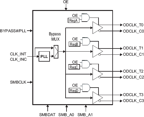
The 9214 clock generator provides the necessary clock signals to support the Rambus XDRTM memory subsystem and Redwood logic interface. The clock source is a reference clock that may or may not be modulated for spread spectrum. The 9214 provides 4 differential clock pairs in a space saving 28-pin TSSOP package and provides an off-the-shelf high-performance interface solution. Figure 1 shows the major components of the 9214 XDR Clock Generator. These include the a PLL, a Bypass Multiplexer and four differential output buffers. The outputs can be disabled by a logic low on the OE pin. An output is enabled by the combination of the OE pin being high, and 1 in its SMBus Output control register bit. The PLL receives a reference clock, CLK_INT/C and outputs a clock signal at a frequency equal to the input frequency times a multiplier. Table 2 shows the multipliers selectable via the SMBus interface. This clock signal is then fed to the differential output buffers to drive the enabled clocks. Disabled outputs are set to Hi-Z. The Bypass mode routes the input clock, CLK_INT/C, directly to the differential output buffers, bypassing the PLL. Up to four 9214 devices can be cascaded on the same SMBus. Table 3 shows the SMBus addressing and control for the four devices.
Documents
Technical documentation and resources


