Deep-Dive with AI
Search across all available documentation for this part.

Deep-Dive with AI
Technical Specifications
Parameters and characteristics for this part
| Specification | SN74AUC2G241YEPR |
|---|---|
| Current - Output High, Low [custom] | 9 mA |
| Current - Output High, Low [custom] | 9 mA |
| Logic Type | Buffer, Non-Inverting |
| Mounting Type | Surface Mount |
| Number of Bits per Element | 1 |
| Number of Elements | 2 |
| Operating Temperature [Max] | 85 °C |
| Operating Temperature [Min] | -40 °C |
| Output Type | 3-State |
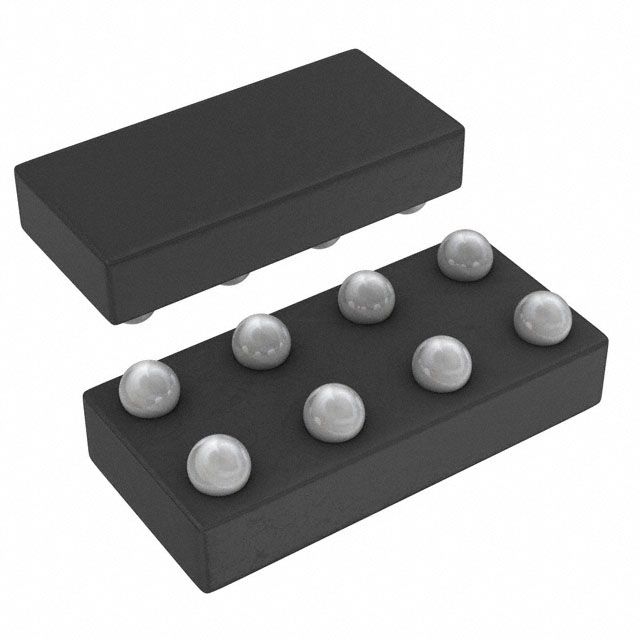
| Package / Case | 8-XFBGA, DSBGA |
| Supplier Device Package | 8-DSBGA |
| Voltage - Supply [Max] | 2.7 V |
| Voltage - Supply [Min] | 0.8 V |
Pricing
Prices provided here are for design reference only. For realtime values and availability, please visit the distributors directly
| Distributor | Package | Quantity | $ | |
|---|---|---|---|---|
Description
General part information
SN74AUC2G241 Series
This dual buffer/driver is operational at 0.8-V to 2.7-V VCC, but is designed specifically for 1.65-V to 1.95-V VCCoperation.
The SN74AUC2G241 is designed specifically to improve the performance and density of 3-state memory address drivers, clock drivers, and bus-oriented receivers and transmitters.
The device is organized as two 1-bit line drivers with separate output-enable (1OE, 2OE) inputs. When 1OEis low or 2OE is high, the device passes data from the A inputs to the Y outputs. When 1OEis high or 2OE is low, the outputs are in the high-impedance state.
Documents
Technical documentation and resources
No documents available


