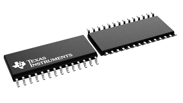
SN75C3238DW
Obsolete3- TO 5.5-V MULTICHANNEL 1MBPS RS-232 LINE DRIVER/RECEIVER WITH +/-15-KV ESD PROTECTION
Deep-Dive with AI
Search across all available documentation for this part.

SN75C3238DW
Obsolete3- TO 5.5-V MULTICHANNEL 1MBPS RS-232 LINE DRIVER/RECEIVER WITH +/-15-KV ESD PROTECTION
Deep-Dive with AI
Technical Specifications
Parameters and characteristics for this part
| Specification | SN75C3238DW |
|---|---|
| Data Rate | 1 Mbps |
| Duplex | Full |
| Mounting Type | Surface Mount |
| Number of Drivers/Receivers [custom] | 5 |
| Number of Drivers/Receivers [custom] | 3 |
| Operating Temperature [Max] | 70 °C |
| Operating Temperature [Min] | 0 °C |
| Package / Case | 28-SOIC |
| Package / Case [x] | 0.295 in |
| Package / Case [y] | 7.5 mm |
| Protocol | RS232 |
| Receiver Hysteresis | 300 mV |
| Supplier Device Package | 28-SOIC |
| Type | Transceiver |
| Voltage - Supply [Max] | 5.5 V |
| Voltage - Supply [Min] | 3 V |
Pricing
Prices provided here are for design reference only. For realtime values and availability, please visit the distributors directly
| Distributor | Package | Quantity | $ | |
|---|---|---|---|---|
| Texas Instruments | TUBE | 1 | $ 3.57 | |
| 100 | $ 3.13 | |||
| 250 | $ 2.19 | |||
| 1000 | $ 1.77 | |||
Description
General part information
SN75C3238E Series
The SN65C3238E and SN75C3238E consist of five line drivers, three line receivers, and a dual charge-pump circuit with ±15-kV ESD (HBM) protection on the driver output (DOUT) and receiver input (RIN) terminals. The devices meet the requirements of TIA/EIA-232-F and provide the electrical interface between notebook and subnotebook computer applications. The charge pump and four small external capacitors allow operation from a single 3-V to 5.5-V supply. In addition, the devices include an always-active noninverting output (ROUT1B), which allows applications using the ring indicator to transmit data while the device is powered down. These devices operate at data signaling rates up to 250 kbit/s and a maximum of 30-V/µs driver output slew rate.
Flexible control options for power management are featured when the serial port and driver inputs are inactive. The auto-powerdown plus feature functions when FORCEON is low andFORCEOFFis high. During this mode of operation, if the devices do not sense valid signal transitions on all receiver and driver inputs for approximately 30 s, the built-in charge pump and drivers are powered down, reducing the supply current to 1 µA. By disconnecting the serial port or placing the peripheral drivers off, auto-powerdown plus occurs if there is no activity in the logic levels for the driver inputs. Auto-powerdown plus can be disabled when FORCEON andFORCEOFFare high. With auto-powerdown plus enabled, the devices activate automatically when a valid signal is applied to any receiver or driver input.INVALIDis high (valid data) if any receiver input voltage is greater than 2.7 V or less than -2.7 V, or has been between -0.3 V and 0.3 V for less than 30 µs.INVALIDis low (invalid data) if all receiver input voltages are between -0.3 V and 0.3 V for more than 30 µs. Refer to Figure 5 for receiver input levels.
The SN65C3238E and SN75C3238E consist of five line drivers, three line receivers, and a dual charge-pump circuit with ±15-kV ESD (HBM) protection on the driver output (DOUT) and receiver input (RIN) terminals. The devices meet the requirements of TIA/EIA-232-F and provide the electrical interface between notebook and subnotebook computer applications. The charge pump and four small external capacitors allow operation from a single 3-V to 5.5-V supply. In addition, the devices include an always-active noninverting output (ROUT1B), which allows applications using the ring indicator to transmit data while the device is powered down. These devices operate at data signaling rates up to 250 kbit/s and a maximum of 30-V/µs driver output slew rate.
Documents
Technical documentation and resources


