Deep-Dive with AI
Search across all available documentation for this part.

Deep-Dive with AI
Technical Specifications
Parameters and characteristics for this part
| Specification | CD4099BM96 |
|---|---|
| Circuit | 1:8 |
| Current - Output High, Low [custom] | 6.8 mA |
| Current - Output High, Low [custom] | 6.8 mA |
| Delay Time - Propagation | 50 ns |
| Independent Circuits | 1 |
| Logic Type | D-Type, Addressable |
| Mounting Type | Surface Mount |
| Operating Temperature [Max] | 125 °C |
| Operating Temperature [Min] | -55 °C |
| Output Type | 1.81 mOhm |
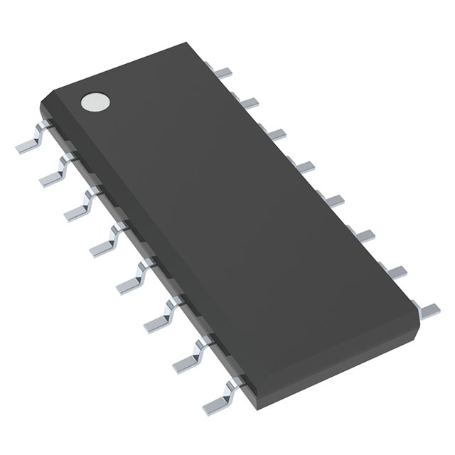
| Package / Case | 16-SOIC |
| Package / Case [x] | 0.154 in |
| Package / Case [y] | 3.9 mm |
| Supplier Device Package | 16-SOIC |
| Voltage - Supply [Max] | 18 V |
| Voltage - Supply [Min] | 3 V |
Pricing
Prices provided here are for design reference only. For realtime values and availability, please visit the distributors directly
| Distributor | Package | Quantity | $ | |
|---|---|---|---|---|
| Digikey | Cut Tape (CT) | 1 | $ 0.61 | |
| 10 | $ 0.53 | |||
| 25 | $ 0.49 | |||
| 100 | $ 0.39 | |||
| 250 | $ 0.36 | |||
| 500 | $ 0.31 | |||
| 1000 | $ 0.24 | |||
| Digi-Reel® | 1 | $ 0.61 | ||
| 10 | $ 0.53 | |||
| 25 | $ 0.49 | |||
| 100 | $ 0.39 | |||
| 250 | $ 0.36 | |||
| 500 | $ 0.31 | |||
| 1000 | $ 0.24 | |||
| Tape & Reel (TR) | 2500 | $ 0.19 | ||
| 5000 | $ 0.18 | |||
| 12500 | $ 0.16 | |||
| 25000 | $ 0.16 | |||
| 62500 | $ 0.15 | |||
| Texas Instruments | LARGE T&R | 1 | $ 0.55 | |
| 100 | $ 0.37 | |||
| 250 | $ 0.29 | |||
| 1000 | $ 0.19 | |||
Description
General part information
CD4099B Series
CD4099B 8-bit addressable latch is a serial-input, parallel-output storage register that can perform a variety of functions.
Data are inputted to a particular bit in the latch when that bit is addressed (by means of input A0, A1, A2) and when WRITE DISABLE is at a low level. When WRITE DISABLE is high, data entry is inhibited; however, all 8 outputs can be continuously read independent of WRITE DISABLE and address inputs.
A master RESET input is available, which resets all bits to a logic "0" level when RESET and WRITE DISABLE are at a high level. When RESET is at a high level, and WRITE RESET is at a low level, the latch acts as a 1-of-8 demultiplexer; the bit that is addressed has an active output which follows the data input, while all unaddressed bits are held to a logic "0" level.
Documents
Technical documentation and resources


