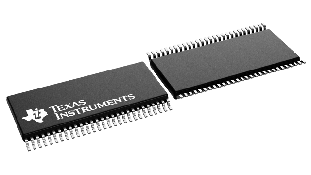
SN74CB3Q16211DGGR
Active3.3-V, 1:1 (SPST), 24-CHANNEL GENERAL-PURPOSE FET BUS SWITCH
Deep-Dive with AI
Search across all available documentation for this part.

SN74CB3Q16211DGGR
Active3.3-V, 1:1 (SPST), 24-CHANNEL GENERAL-PURPOSE FET BUS SWITCH
Deep-Dive with AI
Technical Specifications
Parameters and characteristics for this part
| Specification | SN74CB3Q16211DGGR |
|---|---|
| Circuit [custom] | 1:1 |
| Circuit [custom] | 12 |
| Independent Circuits | 2 |
| Mounting Type | Surface Mount |
| Operating Temperature [Max] | 85 °C |
| Operating Temperature [Min] | -40 °C |
| Package / Case | 6.1 mm |
| Package / Case | 0.24 in |
| Package / Case | 56-TFSOP |
| Supplier Device Package | 56-TSSOP |
| Type | Bus Switch |
| Voltage - Supply [Max] | 3.6 V |
| Voltage - Supply [Min] | 2.3 V |
| Voltage Supply Source | Single Supply |
Pricing
Prices provided here are for design reference only. For realtime values and availability, please visit the distributors directly
| Distributor | Package | Quantity | $ | |
|---|---|---|---|---|
| Digikey | Cut Tape (CT) | 1 | $ 2.68 | |
| 10 | $ 2.41 | |||
| 25 | $ 2.27 | |||
| 100 | $ 1.94 | |||
| 250 | $ 1.82 | |||
| 500 | $ 1.59 | |||
| 1000 | $ 1.32 | |||
| Digi-Reel® | 1 | $ 2.68 | ||
| 10 | $ 2.41 | |||
| 25 | $ 2.27 | |||
| 100 | $ 1.94 | |||
| 250 | $ 1.82 | |||
| 500 | $ 1.59 | |||
| 1000 | $ 1.32 | |||
| Tape & Reel (TR) | 2000 | $ 1.23 | ||
| 6000 | $ 1.18 | |||
| Texas Instruments | LARGE T&R | 1 | $ 2.02 | |
| 100 | $ 1.67 | |||
| 250 | $ 1.20 | |||
| 1000 | $ 0.90 | |||
Description
General part information
SN74CB3Q16211 Series
The SN74CB3Q16211 device is a high-bandwidth FET bus switch utilizing a charge pump to elevate the gate voltage of the pass transistor, providing a low and flat ON-state resistance (ron). The low and flat ON-state resistance allows for minimal propagation delay and supports rail-to-rail switching on the data input/output (I/O) ports. The device also features low data I/O capacitance to minimize capacitive loading and signal distortion on the data bus. Specifically designed to support high-bandwidth applications, the SN74CB3Q16211 device provides an optimized interface solution ideally suited for broadband communications, networking, and data-intensive computing systems.
The SN74CB3Q16211 device is organized as two 12-bit bus switches with separate output-enable (1OE, 2OE) inputs. It can be used as two 12-bit bus switches or as one 24-bit bus switch. WhenOEis low, the associated 12-bit bus switch is ON and the A port is connected to the B port, allowing bidirectional data flow between ports. WhenOEis high, the associated 12-bit bus switch is OFF, and a high-impedance state exists between the A and B ports.
This device is fully specified for partial-power-down applications using Ioff. The Ioffcircuitry prevents damaging current backflow through the device when it is powered down.
Documents
Technical documentation and resources


