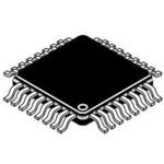
MC100EP195FAR2G
ActiveDELAY LINE IC, PROGRAMMABLE, 1024 TAPS, 10 PS DELAY/ONE TAP, 12.2 NS TOTAL DELAY, 3 V TO 3.6 V, 32 P… MORE
Deep-Dive with AI
Search across all available documentation for this part.

MC100EP195FAR2G
ActiveDELAY LINE IC, PROGRAMMABLE, 1024 TAPS, 10 PS DELAY/ONE TAP, 12.2 NS TOTAL DELAY, 3 V TO 3.6 V, 32 P… MORE
Deep-Dive with AI
Technical Specifications
Parameters and characteristics for this part
| Specification | MC100EP195FAR2G |
|---|---|
| Available Total Delays [Max] | 12.2 ns |
| Available Total Delays [Min] | 2.2 ns |
| Delay to 1st Tap | 2.2 ns |
| Function | Programmable |
| Mounting Type | Surface Mount |
| Number of Independent Delays | 1 |
| Number of Taps/Steps | 1024 |
| Operating Temperature [Max] | 85 °C |
| Operating Temperature [Min] | -40 °C |
| Package / Case | 32-LQFP |
| Supplier Device Package | 32-LQFP (7x7) |
| Tap Increment | 10 ps |
| Voltage - Supply [Max] | 3.6 V |
| Voltage - Supply [Min] | 3 V |
Pricing
Prices provided here are for design reference only. For realtime values and availability, please visit the distributors directly
Description
General part information
MC100EP195 Series
NECL/PECL input transition.The delay section consists of a programmable matrix of gates and multiplexers as shown in the data sheet logic diagram. The delay increment of the EP195 has a digitally selectable resolution of about 10 ps and a range of up to 10.2 ns. The required delay is selected by the 10 data select inputs D(0:9) which are latched on chip by a high signal on the latch enable (LEN) control. The MC10/100EP195 is a programmable delay chip (PDC) designed primarily for clock deskewing and timing adjustment. It provides variable delay of a differential The approximate delay values for varying tap numbers correlating to D0 (LSB) through D9 (MSB) are shown in the data sheet.Because the EP195 is designed using a chain of multiplexers it has a fixed minimum delay of 2.2 ns. An additional pin D10 is provided for cascading multiple PDCs for increased programmable range. The cascade logic allows full control of multiple PDCs.Select input pins D0-D10 may be threshold controlled by combinations of interconnects between VEF(pin 7) and VCF(pin 8) for CMOS, ECL, or TTL level signals. For CMOS input levels, leave VCFand VEFopen. For ECL operation, short VCFand VEF(pins 7 and 8). For TTL level operation, connect a 1.5 V supply reference to VCFand leave open VEFpin. The 1.5 V reference voltage to VCFpin can be accomplished by placing a 1.5k Ohm or 500 Ohm resistor between VCFand VEEfor 3.3 V or 5.0 V power supplies, respectively.The VBBpin, an internally generated voltage supply, is available to this device only. For single-ended input conditions, the unused differential input is connected to VBBas a switching reference voltage. VBBmay also rebias AC coupled inputs. When used, decouple VBBand VCCvia a 0.01 uF capacitor and limit current sourcing or
Documents
Technical documentation and resources


