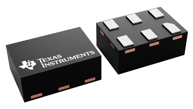
TPS62730DRYR
ActiveSTEP DOWN CONVERTER WITH BYPASS MODE FOR ULTRA LOW POWER WIRELESS APPLICATIONS
Deep-Dive with AI
Search across all available documentation for this part.

TPS62730DRYR
ActiveSTEP DOWN CONVERTER WITH BYPASS MODE FOR ULTRA LOW POWER WIRELESS APPLICATIONS
Deep-Dive with AI
Technical Specifications
Parameters and characteristics for this part
| Specification | TPS62730DRYR |
|---|---|
| Applications | Converter, Bluetooth (BLT) |
| Mounting Type | Surface Mount |
| Number of Outputs | 1 |
| Operating Temperature [Max] | 85 °C |
| Operating Temperature [Min] | -40 C |
| Package / Case | 6-UFDFN |
| Supplier Device Package | 6-SON (1.45x1) |
| Voltage - Input [Max] | 3.9 V |
| Voltage - Input [Min] | 1.9 V |
| Voltage - Output | 2.1 V |
Pricing
Prices provided here are for design reference only. For realtime values and availability, please visit the distributors directly
| Distributor | Package | Quantity | $ | |
|---|---|---|---|---|
| Digikey | Cut Tape (CT) | 1 | $ 1.42 | |
| 10 | $ 1.27 | |||
| 25 | $ 1.20 | |||
| 100 | $ 0.99 | |||
| 250 | $ 0.93 | |||
| 500 | $ 0.82 | |||
| 1000 | $ 0.65 | |||
| 2500 | $ 0.60 | |||
| Digi-Reel® | 1 | $ 1.42 | ||
| 10 | $ 1.27 | |||
| 25 | $ 1.20 | |||
| 100 | $ 0.99 | |||
| 250 | $ 0.93 | |||
| 500 | $ 0.82 | |||
| 1000 | $ 0.65 | |||
| 2500 | $ 0.60 | |||
| N/A | 16126 | $ 1.40 | ||
| Tape & Reel (TR) | 5000 | $ 0.57 | ||
| 10000 | $ 0.55 | |||
| Texas Instruments | LARGE T&R | 1 | $ 1.05 | |
| 100 | $ 0.81 | |||
| 250 | $ 0.60 | |||
| 1000 | $ 0.43 | |||
Description
General part information
TPS62730 Series
The TPS62730 is a high frequency synchronous step-down DC-DC converter optimized for ultra low-power wireless applications. The device is optimized to supply TI’s Low-Power Wireless sub 1-GHz and 2.4-GHz RF transceivers and System-On-Chip (SoC) solutions. The TPS62730 reduces the current consumption drawn from the battery during TX and RX mode by a high efficient step-down voltage conversion. The device provides an output current of up to 100 mA and allows the use of tiny and low-cost chip inductors and capacitors. With an input voltage range of 1.9 V to 3.9 V, the device supports Li-primary battery chemistries such as Li-SOCl2, Li-SO2, Li-MnO2, and also two cell alkaline batteries.
The TPS62730 features an Ultra Low-Power bypass mode with typical 30-nA current consumption to support sleep and low power modes of TI’s CC2540BluetoothLow Energy and CC430 SoC solutions. In this bypass mode, the output capacitor of the DC-DC converter is connected through an integrated typical 2.1-Ω bypass switch to the battery.
In DC-DC operation mode the device provides a fixed output voltage to the system. With a switch frequency up to 3 MHz, the TPS62730 features low output ripple voltage and low noise even with a small 2.2-µF output capacitor. The automatic transition into bypass mode during DC-DC operation prevents an increase of output ripple voltage and noise once the DC-DC converter operates close to 100% duty cycle. The device automatically enters bypass mode once the battery voltage falls below the transition threshold VIT BYP. The TPS62730 is available in a 1 × 1.5-mm26-pin USON package.
Documents
Technical documentation and resources


