Deep-Dive with AI
Search across all available documentation for this part.

Technical Specifications
Parameters and characteristics for this part
| Specification | SN74LVC2GU04DCKT |
|---|---|
| Current - Output High, Low [x] | 32 mA |
| Current - Output High, Low [y] | 32 mA |
| Current - Quiescent (Max) [Max] | 10 µA |
| Input Logic Level - High [Max] | 4.13 V |
| Input Logic Level - High [Min] | 1.24 V |
| Input Logic Level - Low [Max] | 1.38 V |
| Input Logic Level - Low [Min] | 0.41 V |
| Logic Type | Inverter |
| Max Propagation Delay @ V, Max CL [Max] | 3.5 ns |
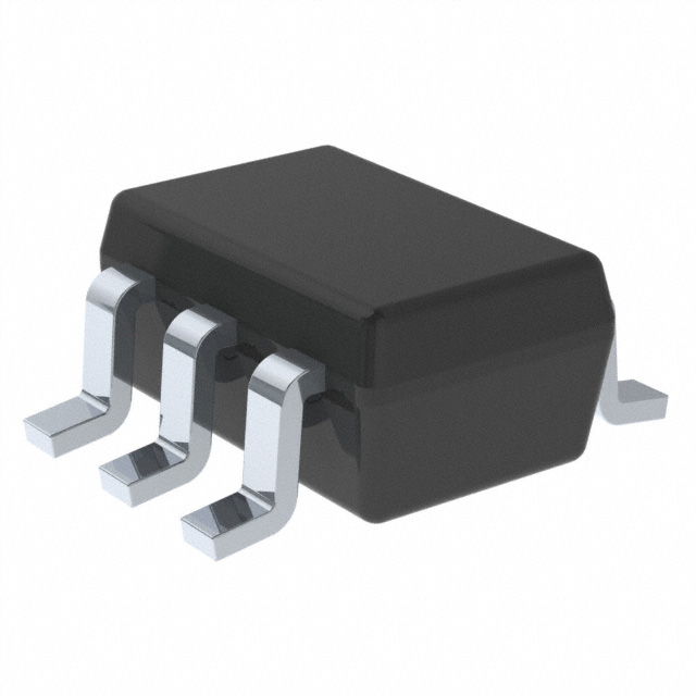
| Mounting Type | Surface Mount |
| Number of Circuits | 2 |
| Number of Inputs | 2 |
| Operating Temperature [Max] | 125 °C |
| Operating Temperature [Min] | -40 °C |
| Package / Case | 6-TSSOP, SC-88, SOT-363 |
| Supplier Device Package | SC-70-6 |
| Voltage - Supply [Max] | 5.5 V |
| Voltage - Supply [Min] | 1.65 V |
Pricing
Prices provided here are for design reference only. For realtime values and availability, please visit the distributors directly
| Distributor | Package | Quantity | $ | |
|---|---|---|---|---|
| Digikey | Cut Tape (CT) | 1 | $ 1.26 | |
| 10 | $ 1.13 | |||
| 25 | $ 1.07 | |||
| 100 | $ 0.88 | |||
| Digi-ReelÛ | 1 | $ 1.26 | ||
| 10 | $ 1.13 | |||
| 25 | $ 1.07 | |||
| 100 | $ 0.88 | |||
| Tape & Reel (TR) | 250 | $ 0.82 | ||
| 500 | $ 0.73 | |||
| 1250 | $ 0.57 | |||
| 2500 | $ 0.53 | |||
| 6250 | $ 0.51 | |||
| 12500 | $ 0.49 | |||
| Texas Instruments | SMALL T&R | 1 | $ 1.08 | |
| 100 | $ 0.74 | |||
| 250 | $ 0.57 | |||
| 1000 | $ 0.38 | |||
Description
General part information
SN74LVC2GU04 Series
This dual inverter is designed for 1.65-V to 5.5-V VCCoperation.
The SN74LVC2GU04 device contains two inverters with unbuffered outputs and performs the Boolean function Y =A.
NanoFree™ package technology is a major breakthrough in IC packaging concepts, using the die as the package.
Documents
Technical documentation and resources


