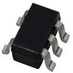
NLV74VHC1GT86DTT1G
ObsoleteXOR GATE 1-ELEMENT 2-IN CMOS 5-PIN TSOP T/R AUTOMOTIVE AEC-Q100
Deep-Dive with AI
Search across all available documentation for this part.

NLV74VHC1GT86DTT1G
ObsoleteXOR GATE 1-ELEMENT 2-IN CMOS 5-PIN TSOP T/R AUTOMOTIVE AEC-Q100
Deep-Dive with AI
Technical Specifications
Parameters and characteristics for this part
| Specification | NLV74VHC1GT86DTT1G |
|---|---|
| Current - Output High, Low [custom] | 8 mA |
| Current - Output High, Low [custom] | 8 mA |
| Current - Quiescent (Max) [Max] | 1 çA |
| Grade | Automotive |
| Input Logic Level - High [Max] | 4.4 V |
| Input Logic Level - High [Min] | 2.9 V |
| Input Logic Level - Low [Max] | 0.36 V |
| Input Logic Level - Low [Min] | 0.1 V |
| Logic Type | XOR (Exclusive OR) |
| Max Propagation Delay @ V, Max CL | 8.8 ns |
| Mounting Type | Surface Mount |
| Number of Circuits | 1 |
| Number of Inputs | 2 |
| Operating Temperature [Max] | 125 °C |
| Operating Temperature [Min] | -55 °C |
| Package / Case | SOT-23-5 Thin, TSOT-23-5 |
| Qualification | AEC-Q100 |
| Supplier Device Package | 5-TSOP |
| Voltage - Supply [Max] | 5.5 V |
| Voltage - Supply [Min] | 3 V |
Pricing
Prices provided here are for design reference only. For realtime values and availability, please visit the distributors directly
| Distributor | Package | Quantity | $ | |
|---|---|---|---|---|
Description
General part information
NLV74VHC1GT86 Series
The NLV74VHC1GT86 is an advanced high speed CMOS 2-input Exclusive OR gate fabricated with silicon gate CMOS technology. It achieves high speed operation similar to equivalent Bipolar SchottkyTTL while maintaining CMOS low power dissipation.The internal circuit is composed of three stages, including a buffer output which provides high noise immunity and stable output.The device input is compatible with TTL-type input thresholds andthe output has a full 5V CMOS level output swing. The input protection circuitry on this device allows overvoltage tolerance on the input,allowing the device to be used as a logic-level translator from 3.0V CMOS logic to 5.0V CMOS Logic or from 1.8V CMOS logic to 3.0V CMOS Logic while operating at the high-voltage power supply.The NLV74VHC1GT86 input structure provides protection when voltages up to 5.5V are applied, regardless of the supply voltage. This allows the NLV74VHC1GT86 to be used to interface 5V circuits to 3V circuits. The output structures also provide protection when VCC= 0V.These input and output structures help prevent device destruction caused by supply voltage - input/output voltage mismatch, battery backup, hot insertion, etc.
Documents
Technical documentation and resources


