Deep-Dive with AI
Search across all available documentation for this part.

Deep-Dive with AI
Technical Specifications
Parameters and characteristics for this part
| Specification | MM74HCT541SJ |
|---|---|
| Current - Output High, Low | 7.2 mA, 7.2 mA |
| Logic Type | Buffer, Non-Inverting |
| Mounting Type | Surface Mount |
| Number of Bits per Element | 8 |
| Number of Elements | 1 |
| Operating Temperature [Max] | 85 °C |
| Operating Temperature [Min] | -40 °C |
| Output Type | 3-State |
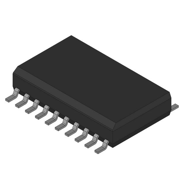
| Package / Case | 20-SOIC |
| Package / Case | 0.209 " |
| Package / Case | 5.3 mm |
| Supplier Device Package | 20-SOP |
| Voltage - Supply [Max] | 5.5 V |
| Voltage - Supply [Min] | 4.5 V |
Pricing
Prices provided here are for design reference only. For realtime values and availability, please visit the distributors directly
| Distributor | Package | Quantity | $ | |
|---|---|---|---|---|
| Digikey | Tube | 1158 | $ 0.26 | |
| 1158 | $ 0.26 | |||
Description
General part information
MC74HCT541A Series
The MM74HCT540 and MM74HCT541 3-STATE buffers utilize advanced silicon-gate CMOS technology and are general purpose high speed inverting and non-inverting buffers. They possess high drive current outputs which enable high speed operation even when driving large bus capacitances. These circuits achieve speeds comparable to low power Schottky devices, while retaining the low power consumption of CMOS. Both devices are TTL input compatible and have a fanout of 15 LS-TTL equivalent inputs. MM74HCT devices are intended to interface between TTL and NMOS components and standard CMOS devices. These parts are also plug-in replacements for LS-TTL devices and can be used to reduce power consumption in existing designs. The MM74HCT540 is an inverting buffer and the MM74HCT541 is a non-inverting buffer. The 3-STATE control gate operates as a two-input NOR such that if either G1# or G2# are HIGH, all eight outputs are in the high-impedance state. In order to enhance PC board layout, the MM74HCT540 and MM74HCT541 offers a pinout having inputs and outputs on opposite sides of the package. All inputs are protected from damage due to static discharge by diodes to VCCand ground.
Documents
Technical documentation and resources


