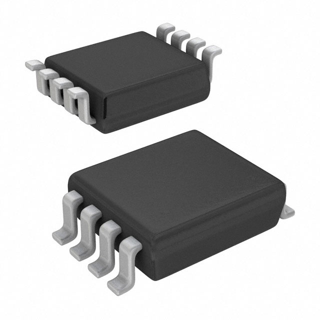
FSUSB46K8X
ObsoleteHI-SPEED USB2.0 (480MBPS) DPST SWITCH WITH DEDICATED CHARGER PORT DETECTION
Deep-Dive with AI
Search across all available documentation for this part.

FSUSB46K8X
ObsoleteHI-SPEED USB2.0 (480MBPS) DPST SWITCH WITH DEDICATED CHARGER PORT DETECTION
Deep-Dive with AI
Technical Specifications
Parameters and characteristics for this part
| Specification | FSUSB46K8X |
|---|---|
| -3db Bandwidth | 720 MHz |
| Applications | USB |
| Features | Break-Before-Make, USB 2.0 |
| Mounting Type | Surface Mount |
| Multiplexer/Demultiplexer Circuit | 2:1 |
| Number of Channels | 1 |
| On-State Resistance (Max) [Max] | 6.5 Ohm |
| Operating Temperature [Max] | 85 °C |
| Operating Temperature [Min] | -40 °C |
| Package / Case | 8-VFSOP |
| Package / Case [y] | 2.3 mm |
| Package / Case [y] | 0.091 in |
| Supplier Device Package | US8 |
| Switch Circuit | DPST |
| Voltage - Supply, Single (V+) [Max] | 4.3 V |
| Voltage - Supply, Single (V+) [Min] | 3 V |
Pricing
Prices provided here are for design reference only. For realtime values and availability, please visit the distributors directly
| Distributor | Package | Quantity | $ | |
|---|---|---|---|---|
Description
General part information
FSUSB46 Series
The FSUSB45 is a bi-directional, low-power, two-port, Hi-Speed, USB2.0 switch. Configured as a double-pole, double-throw (DPDT) switch, it is optimized for switching between two Hi-Speed (480Mbps) sources or a Hi-Speed source and a Full-Speed (12Mbps) source. The FSUSB45 is compatible with the requirements of USB2.0 and features an extremely low on capacitance (CON) of 7.0pF. The wide bandwidth of this device (720MHz) exceeds the bandwidth needed to pass the third harmonic, resulting in signals with minimum edge and phase distortion. Superior channel-to-channel crosstalk also minimizes interference. The FSUSB45 contains special circuitry on the switch I/O pins for applications where the VCCsupply is powered-off (VCC=0), which allows the device to withstand an over-voltage condition. This device is designed to minimize current consumption even when the control voltage applied to the SEL pin is lower than the supply voltage (VCC). This feature is especially valuable to mobile applications, such as cell phones, allowing for direct interface with the general-purpose I/Os of the baseband processor. An additional feature is the detection of the 1,1 state on D+/D- to signal an interrupt (INT) to the processor when entering a dedicated charging port mode of operation.
Documents
Technical documentation and resources


