Zenode.ai Logo
Beta
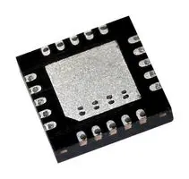
MICROCHIP PIC16F15345-E/GZ
Integrated Circuits (ICs)

BD3508MUV-E2

Active
Rohm Semiconductor

3A VARIABLE OUTPUT, HIGH-ACCURACY LDO REGULATOR

Deep-Dive with AI

Search across all available documentation for this part.

MICROCHIP PIC16F15345-E/GZ
Integrated Circuits (ICs)

BD3508MUV-E2

Active
Rohm Semiconductor

3A VARIABLE OUTPUT, HIGH-ACCURACY LDO REGULATOR

Technical Specifications

Parameters and characteristics for this part

SpecificationBD3508MUV-E2
Control FeaturesSoft Start, Enable
Current - Output3 A
Mounting TypeSurface Mount
Number of Regulators1
Output ConfigurationPositive
Output TypeAdjustable
Package / Case20-VFQFN Exposed Pad
Protection FeaturesOver Current, Under Voltage Lockout (UVLO), Over Temperature
Supplier Device Package20-VQFN
Voltage - Input (Max) [Max]4.5 V
Voltage - Output (Max) [Max]2.7 V
Voltage - Output (Min/Fixed)0.65 V
Voltage Dropout (Max)0.1 V

Pricing

Prices provided here are for design reference only. For realtime values and availability, please visit the distributors directly

DistributorPackageQuantity$
DigikeyN/A 0$ 0.99
NewarkEach (Supplied on Cut Tape) 1$ 1.53

Description

General part information

BD3508MUV Series

The BD3508MUV ultra low-dropout linear chipset regulator operates from a very low input supply, and offers ideal performance in low input voltage to low output voltage applications. It incorporates a built-in N-MOSFET power transistor to minimize the input-to-output voltage differential to the ON resistance (RONMAX=100mO) level. By lowering the dropout voltage in this way, the regulator realizes high current output (Iomax=3.0A) with reduced conversion loss, and thereby obviates the switching regulator and its power transistor, choke coil, and rectifier diode. Thus, the BD3508MUV is designed to enable significant package profile downsizing and cost reduction. An external resistor allows the entire range of output voltage configurations between 0.65 and 2.7V, while the NRCS (soft start) function enables a controlled output voltage ramp-up, which can be programmed to whatever power supply sequence is required.

Documents

Technical documentation and resources

Technical Data Sheet EN

Datasheet

Solder Joint Rate and Thermal Resistance of Exposed Pad

Thermal Design

Problem Situations: Power Supply Does Not Start

Schematic Design & Verification

Factory Information

Manufacturing Data

Impedance Characteristics of Bypass Capacitor

Schematic Design & Verification

Design Guide and Example of Stencil for Exposed Pad

Thermal Design

Method for Calculating Junction Temperature from Transient Thermal Resistance Data

Thermal Design

Connecting LDOs in Parallel

Schematic Design & Verification

VQFN020V4040 Package Information

Package Information

UL94 Flame Classifications of Mold Compound

Environmental Data

What Is Thermal Design

Thermal Design

Six Steps for Successful Thermal Design of LDO Regulator ICs

White Paper

Thermal Resistance

Thermal Design

Calculating Junction Temperature from Inrush Current

Thermal Design

Table of resistance for output voltage setting on linear regulator Ics

Schematic Design & Verification

θ<sub>JA</sub> and Ψ<sub>JT</sub>

Thermal Design

Basics of Thermal Resistance and Heat Dissipation

Thermal Design

Reverse Voltage Protection

Schematic Design & Verification

Anti-Whisker formation

Package Information

EMC Measures for LDOs

Schematic Design & Verification

Precautions When Measuring the Rear of the Package with a Thermocouple

Thermal Design

Measurement Method for Phase Margin with Frequency Response Analyzer (FRA)

Schematic Design & Verification

Five Steps for Successful Thermal Design of IC

White Paper

Simple Test Method for Estimating the Stability of Linear Regulators

Schematic Design & Verification

Overview of ROHM's Simulation Models(for ICs and Discrete Semiconductors)

Technical Article

Heat Dissipation Effect of Thermal Via in Exposed Pad Type Package

Thermal Design

θ<sub>JC</sub> and Ψ<sub>JT</sub>

Thermal Design

Power Supply Sequence Circuit with General Purpose Power Supply IC

Schematic Design & Verification

PCB Layout Thermal Design Guide

Thermal Design

Suppression Method of Switching Noise Using Linear Regulator and Low Pass Filter

Schematic Design & Verification

How to Use the Two-Resistor Model

Thermal Design

Judgment Criteria of Thermal Evaluation

Thermal Design

Thermal Calculation for Linear Regulator

Thermal Design

Usage of SPICE Macromodel (for LDO)

Schematic Design & Verification

How to Select Reverse Current Protection Diodes for LDO Regulators

Schematic Design & Verification

Power Source ON/OFF Characteristics for Linear Regulator

Schematic Design & Verification

Basics of Linear Regulators

Schematic Design & Verification

Compliance with the ELV directive

Environmental Data

How to Use the Thermal Resistance and Thermal Characteristics Parameters

Thermal Design