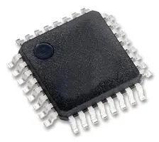
MC100LVEP210FAG
ActiveCLOCK DRIVER, 1:5 DIFFERENTIAL, DUAL ECL / PECL / HSTL, 2.5 V / 3.3 V
Deep-Dive with AI
Search across all available documentation for this part.

MC100LVEP210FAG
ActiveCLOCK DRIVER, 1:5 DIFFERENTIAL, DUAL ECL / PECL / HSTL, 2.5 V / 3.3 V
Deep-Dive with AI
Technical Specifications
Parameters and characteristics for this part
| Specification | MC100LVEP210FAG |
|---|---|
| Differential - Input:Output [custom] | True |
| Differential - Input:Output [custom] | True |
| Frequency - Max [Max] | 3 GHz |
| Input | LVDS, HSTL, ECL, PECL |
| Mounting Type | Surface Mount |
| Number of Circuits | 2 |
| Operating Temperature [Max] | 85 °C |
| Operating Temperature [Min] | -40 °C |
| Output | ECL, PECL |
| Package / Case | 32-LQFP |
| Ratio - Input:Output | 1:5 |
| Supplier Device Package | 32-LQFP (7x7) |
| Type | Fanout Buffer (Distribution) |
| Voltage - Supply [Max] | 3.8 V |
| Voltage - Supply [Min] | 2.375 V |
Pricing
Prices provided here are for design reference only. For realtime values and availability, please visit the distributors directly
Description
General part information
MC100LVEP210 Series
The MC100LVEL39 is a low skew 2/4, 4/6 clock generation chip designed explicitly for low skew clock generation applications. The internal dividers are synchronous to each other, therefore, the common output edges are all precisely aligned. The device can be driven by either a differential or single-ended input signal. In addition, by using the VBB output, a sinusoidal source can be AC coupled into the device.The common enable (ENbar) is synchronous so that the internal dividers will only be enabled/disabled when the internal clock is already in the LOW state. This avoids any chance of generating a runt clock pulse on the internal clock when the device is enabled/disabled as can happen with an asynchronous control. An internal runt pulse could lead to losing synchronization between the internal divider stages. The internal enable flip-flop is clocked on the falling edge of the input clock, therefore, all associated specification limits are referenced to the negative edge of the clock input.Upon startup, the internal flip-flops will attain a random state; therefore, for systems which utilize multiple LVEL39s, the master reset (MR) input must be asserted to ensure synchronization. For systems which only use one LVEL39, the MR pin need not be exercised as the internal divider design ensures synchronization between the 2/4 and the 4/6 outputs of a single device.The VBBpin, an internally generated voltage supply, is available to this device only. For single-ended input conditions, the unused differential input is connected to VBBas a switching reference voltage. VBBmay also rebias AC coupled inputs. When used, decouple VBBand VCCvia a 0.01 F capacitor and limit current sourcing or sinking to 0.5 mA. When not used, VBBshould be left open.
Documents
Technical documentation and resources


