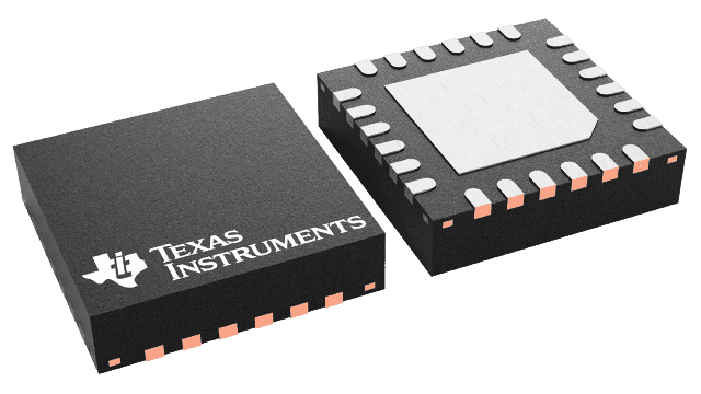
DAC9881SRGET
Active18-BIT, SINGLE-CHANNEL, LOW-NOISE, VOLTAGE OUTPUT DAC FOR HIGH ACCURACY APPLICATIONS
Deep-Dive with AI
Search across all available documentation for this part.

DAC9881SRGET
Active18-BIT, SINGLE-CHANNEL, LOW-NOISE, VOLTAGE OUTPUT DAC FOR HIGH ACCURACY APPLICATIONS
Technical Specifications
Parameters and characteristics for this part
| Specification | DAC9881SRGET |
|---|---|
| Architecture | R-2R |
| Data Interface | DSP, SPI |
| Differential Output | False |
| INL/DNL (LSB) | 2.5 LSB, 1 LSB |
| Mounting Type | Surface Mount |
| Operating Temperature [Max] | 105 ░C |
| Operating Temperature [Min] | -40 °C |
| Output Type | Voltage - Buffered |
| Package / Case | 24-VFQFN Exposed Pad |
| Reference Type | External |
| Settling Time | 5 µs |
| Supplier Device Package | 24-VQFN (4x4) |
| Voltage - Supply, Analog | 5 V |
| Voltage - Supply, Analog [Max] | 3.3 V |
| Voltage - Supply, Analog [Min] | 2.7 V |
| Voltage - Supply, Digital [Max] | 5.5 V |
| Voltage - Supply, Digital [Min] | 1.7 V |
Pricing
Prices provided here are for design reference only. For realtime values and availability, please visit the distributors directly
| Distributor | Package | Quantity | $ | |
|---|---|---|---|---|
| Digikey | Cut Tape (CT) | 1 | $ 35.79 | |
| 10 | $ 33.01 | |||
| 25 | $ 31.52 | |||
| 100 | $ 28.18 | |||
| Digi-Reel® | 1 | $ 35.79 | ||
| 10 | $ 33.01 | |||
| 25 | $ 31.52 | |||
| 100 | $ 28.18 | |||
| Tape & Reel (TR) | 250 | $ 26.89 | ||
| Texas Instruments | SMALL T&R | 1 | $ 28.09 | |
| 100 | $ 24.97 | |||
| 250 | $ 20.52 | |||
| 1000 | $ 18.36 | |||
Description
General part information
DAC9881 Series
The DAC9881 is an 18-bit, single-channel, voltage-output digital-to-analog converter (DAC). The device features 18-bit monotonicity, excellent linearity, very low-noise, and fast settling time. The on-chip precision output amplifier allows for a rail-to-rail output swing to be achieved over the full supply range of 2.7 V to 5.5 V.
The device supports a standard serial peripheral interface (SPI) capable of operating with input data clock frequencies of up to 50 MHz. The DAC9881 requires an external reference voltage to set the output range of the DAC channel. A programmable power-on reset circuit is also incorporated into the device to make sure that the DAC output powers up at zero-scale or midscale, and remains there until a valid write command.
Additionally, the DAC9881 has the capability to function in either unipolar straight binary or two’s complement mode. The DAC9881 provides low-power operation. To further save energy, power-down mode can be achieved by accessing the PDN pin, thereby reducing the current consumption to 25 µA at 5 V. Power consumption is 4 mW at 5 V, reducing to 125 µW in power-down mode.
Documents
Technical documentation and resources


