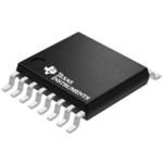
DAC1280IPWR
ActiveVERY LOW DISTORTION DIGITAL-TO-ANALOG CONVERTER FOR SEISMIC APPLICATIONS
Deep-Dive with AI
Search across all available documentation for this part.

DAC1280IPWR
ActiveVERY LOW DISTORTION DIGITAL-TO-ANALOG CONVERTER FOR SEISMIC APPLICATIONS
Technical Specifications
Parameters and characteristics for this part
| Specification | DAC1280IPWR |
|---|---|
| Data Interface | Serial |
| Mounting Type | Surface Mount |
| Number of Channels | 1 |
| Operating Temperature [Max] | 125 °C |
| Operating Temperature [Min] | -40 °C |
| Package / Case | 16-TSSOP |
| Package / Case [x] | 0.173 in |
| Package / Case [y] | 4.4 mm |
| Supplier Device Package | 16-TSSOP |
| Type | DAC |
| Voltage - Supply | 5 V, 2.5 V |
| Voltage - Supply [Max] | 3.3 V |
| Voltage - Supply [Min] | 1.8 V |
| Voltage Supply Source | Analog and Digital, Dual ± |
Pricing
Prices provided here are for design reference only. For realtime values and availability, please visit the distributors directly
| Distributor | Package | Quantity | $ | |
|---|---|---|---|---|
| Digikey | Cut Tape (CT) | 1 | $ 44.75 | |
| Digi-Reel® | 1 | $ 44.75 | ||
| Tape & Reel (TR) | 2000 | $ 31.00 | ||
| Texas Instruments | LARGE T&R | 1 | $ 37.87 | |
| 100 | $ 33.66 | |||
| 250 | $ 27.67 | |||
| 1000 | $ 24.75 | |||
Description
General part information
DAC1280 Series
The DAC1280 is a very low distortion digital-to-analog converter (DAC) suited for performance testing of seismic equipment. The DAC1280 provides a high-accuracy output signal from a bitstream input. The device achieves very high linearity in a small package while dissipating only 18mW. Together with the high-performance ADS1281 and ADS1282 analog-to-digital converters (ADCs), these devices create a test and measurement system that meets the exacting demands of energy exploration and seismic monitoring equipment.
The DAC1280 is designed to match the system components (power supply, clock and reference voltage) of the companion ADCs, the ADS1281 and ADS1282. The input to the DAC1280 is a 1s density modulated bitstream. The DAC1280 output is a differential current intended for use with an active I/V converter. The I/V converter provides a voltage output suitable for performance testing of sensors and ADCs.
Three gain control pins set the output range in 6dB steps from 0dB to –36db (±2.5V to ±0.039V differential). The attenuation ranges match the gains of the ADS1282 for testing at all gains. The DAC uses a reference voltage and bias resistor to set the full-scale output. The resistor can be adjusted to fine-trim the DAC full-scale.
Documents
Technical documentation and resources


