Deep-Dive with AI
Search across all available documentation for this part.

Deep-Dive with AI
Technical Specifications
Parameters and characteristics for this part
| Specification | OPA2835IDGSEVM |
|---|---|
| -3db Bandwidth | 56 MHz |
| Amplifier Type | Voltage Feedback |
| Board Type | Fully Populated |
| Channels per IC | 2 - Dual |
| Current - Output / Channel [custom] | 40 mA |
| Current - Supply (Main IC) | 250 µA |
| Output Type | Rail-to-Rail |
| Slew Rate | 260 V/µs |
| Supplied Contents | Board(s) |
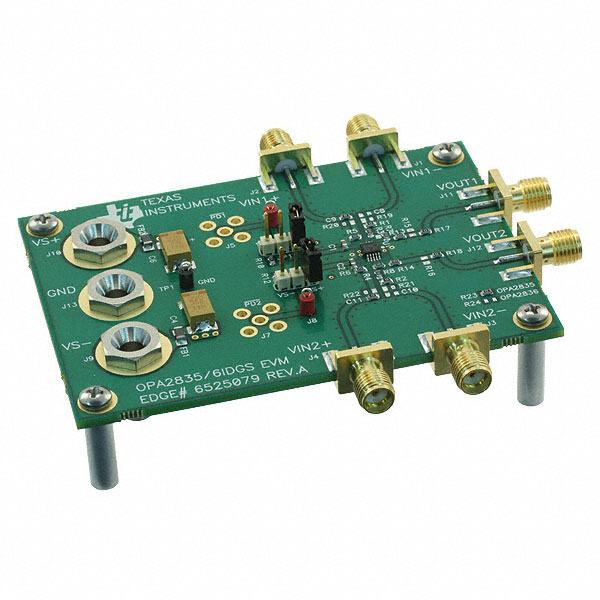
| Utilized IC / Part | OPA2835 |
| Voltage - Supply, Single/Dual (±) [Max] | 5.5 V, 2.75 V |
| Voltage - Supply, Single/Dual (±) [Min] | 2.5 V, -1.25 V |
Pricing
Prices provided here are for design reference only. For realtime values and availability, please visit the distributors directly
| Distributor | Package | Quantity | $ | |
|---|---|---|---|---|
| Digikey | Box | 1 | $ 178.80 | |
Description
General part information
OPA2835 Series
The OPA835 and OPA2835 devices (OPAx835) are single and dual ultra-low-power, rail-to-rail output, negative-rail input, voltage-feedback (VFB) operational amplifiers designed to operate over a power supply range of 2.5-V to 5.5-V with a single supply, or ±1.25-V to ±2.75-V with a dual supply. Consuming only 250 µA per channel and with a unity gain bandwidth of 56 MHz, these amplifiers set an industry-leading performance-to-power ratio for rail-to-rail amplifiers.
For battery-powered, portable applications where power is of key importance, the low power consumption and high-frequency performance of the OPA835 and OPA2835 devices offers performance versus power that is not attainable in other devices. Coupled with a power-savings mode to reduce current to < 1.5 µA, these devices offer an attractive solution for high-frequency amplifiers in battery-powered applications.
The OPA835 RUN package option includes integrated gain-setting resistors for the smallest possible footprint on a printed-circuit-board (approximately 2.00 mm × 2.00 mm). By adding circuit traces on the PCB, gains of +1, –1, –1.33, +2, +2.33, –3, +4, –4, +5, –5.33, +6.33, –7, +8 and inverting attenuations of –0.1429, –0.1875, –0.25, –0.33, –0.75 can be achieved. See Table 9-1 and Table 9-2 for details.
Documents
Technical documentation and resources


