Zenode.ai Logo
Beta
Product thumbnail image
Integrated Circuits (ICs)

BD9E203FP4-ZTL

Active
Rohm Semiconductor

4.5V TO 28V INPUT, 2.0A INTEGRATED MOSFET SINGLE SYNCHRONOUS BUCK DC/DC CONVERTER

Deep-Dive with AI

Search across all available documentation for this part.

Product thumbnail image
Integrated Circuits (ICs)

BD9E203FP4-ZTL

Active
Rohm Semiconductor

4.5V TO 28V INPUT, 2.0A INTEGRATED MOSFET SINGLE SYNCHRONOUS BUCK DC/DC CONVERTER

Technical Specifications

Parameters and characteristics for this part

SpecificationBD9E203FP4-ZTL
Current - Output2 A
Frequency - Switching350 kHz
FunctionStep-Down
Mounting TypeSurface Mount
Number of Outputs1
Operating Temperature [Max]85 °C
Operating Temperature [Min]-40 C
Output ConfigurationPositive
Output TypeAdjustable
Package / CaseSOT-23-6 Thin, TSOT-23-6
Supplier Device PackageTSOT-23-6CJ
Synchronous RectifierTrue
TopologyBuck
Voltage - Input (Max) [Max]28 V
Voltage - Input (Min) [Min]4.5 V
Voltage - Output (Max) [Max]22.4 V
Voltage - Output (Min/Fixed) [Min]0.7 V

Pricing

Prices provided here are for design reference only. For realtime values and availability, please visit the distributors directly

DistributorPackageQuantity$
DigikeyN/A 2105$ 0.88

Description

General part information

BD9E203FP4-Z Series

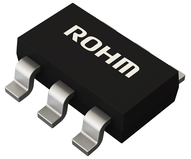
BD9E203FP4-Z is a single synchronous buck DC/DC converter with built-in low on-resistance power MOSFETs. BD9E203FP4-Z is a current mode control. It includes internal phase compensation. It achieves the high power density and offers a small footprint on the PCB by employing small package.

Documents

Technical documentation and resources

What Is Thermal Design

Thermal Design

Phase Compensation Design for Current Mode Buck Converter

Schematic Design & Verification

Two-Resistor Model for Thermal Simulation

Thermal Design

How to Use the Thermal Resistance and Thermal Characteristics Parameters

Thermal Design

PCB Layout Techniques of Buck Converter

Schematic Design & Verification

How to Use the Two-Resistor Model

Thermal Design

Evaluation Board User's Guide for BD9E203FP4-EVK-001

User's Guide

Suppression Method of Switching Noise Using Linear Regulator and Low Pass Filter

Schematic Design & Verification

Step-down DC-DC converter PCB layout EMC Design guide

Schematic Design & Verification

Method for Calculating Junction Temperature from Transient Thermal Resistance Data

Thermal Design

Capacitor Calculation for Buck converter IC

Schematic Design & Verification

BD9E203FP4-Z Data Sheet

Data Sheet

Considering Input Filter to Reduce Conducted Emissions by DCDC Converter

Schematic Design & Verification

Judgment Criteria of Thermal Evaluation

Thermal Design

Overview of ROHM's Simulation Models(for ICs and Discrete Semiconductors)

Technical Article

Bootstrap Circuit in the Buck Converter

Schematic Design & Verification

Resistor Value Table to set Output Voltage of Buck Converter IC

Schematic Design & Verification

Three Steps for Successful Design of DC-DC Converters

White Paper

Snubber Circuit for Buck Converter IC

Schematic Design & Verification

Thermal Resistance

Thermal Design

Efficiency of Buck Converter

Schematic Design & Verification

Design Guide and Example of Stencil for Exposed Pad

Thermal Design

Types of Capacitors Used for Output Smoothing of Switching Regulators and their Precautions

Schematic Design & Verification

Power Supply Sequence Circuit with General Purpose Power Supply IC

Schematic Design & Verification

Five Steps for Successful Thermal Design of IC

White Paper

Method for Determining Constants of Peripheral Parts of Buck DC/DC Converter

Schematic Design & Verification

Diode Selection Method for Asynchronous Converter

Schematic Design & Verification

Calculation of Power Loss (Synchronous)

Schematic Design & Verification

Impedance Characteristics of Bypass Capacitor

Schematic Design & Verification

Calculation of Power Dissipation in Switching Circuit

Schematic Design & Verification

PCB Layout Thermal Design Guide

Thermal Design

Precautions for PCB Layout Regarding Common Mode Filters

Technical Article

The Important Points of Multi-layer Ceramic Capacitor Used in Buck Converter circuit

Schematic Design & Verification

Precautions When Measuring the Rear of the Package with a Thermocouple

Thermal Design

Measurement Method for Phase Margin with Frequency Response Analyzer (FRA)

Schematic Design & Verification

θ<sub>JA</sub> and Ψ<sub>JT</sub>

Thermal Design

Factory Information

Manufacturing Data

PCB Layout Essential Check sheet for Switching Regulator

Schematic Design & Verification

Inductor Calculation for Buck converter IC

Schematic Design & Verification

Heat Dissipation Effect of Thermal Via in Exposed Pad Type Package

Thermal Design

Cutting-Edge Web Simulation Tool "ROHM Solution Simulator" Capable of Complete Circuit Verification of Power Devices and Driver ICs

White Paper

Considerations for Power Inductors Used for Buck Converters

Schematic Design & Verification

TSOT23-6CJ Package Information

Package Information

Considering Polarity of Power Inductor to Reduce Radiated Emission of DC-DC converter

Schematic Design & Verification

Solder Joint Rate and Thermal Resistance of Exposed Pad

Thermal Design

θ<sub>JC</sub> and Ψ<sub>JT</sub>

Thermal Design

Basics of Thermal Resistance and Heat Dissipation

Thermal Design