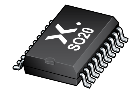
74HC299D-Q100J
Active8-BIT UNIVERSAL SHIFT REGISTER; 3-STATE
Deep-Dive with AI
Search across all available documentation for this part.

74HC299D-Q100J
Active8-BIT UNIVERSAL SHIFT REGISTER; 3-STATE
Deep-Dive with AI
Technical Specifications
Parameters and characteristics for this part
| Specification | 74HC299D-Q100J |
|---|---|
| Function | Universal |
| Grade | Automotive |
| Logic Type | Shift Register |
| Mounting Type | Surface Mount |
| Number of Bits per Element [custom] | 8 |
| Number of Elements | 1 |
| Operating Temperature [Max] | 125 °C |
| Operating Temperature [Min] | -40 °C |
| Output Type | Tri-State |
| Package / Case | 20-SOIC (0.295", 7.50mm Width) |
| Qualification | AEC-Q100 |
| Supplier Device Package | 20-SO |
Pricing
Prices provided here are for design reference only. For realtime values and availability, please visit the distributors directly
| Distributor | Package | Quantity | $ | |
|---|---|---|---|---|
| Digikey | N/A | 1995 | $ 1.47 | |
Description
General part information
74HC299D-Q100 Series
The 74HC299-Q100 is an 8-bit universal shift register with 3-state outputs. It contains eight edge-triggered D-type flip-flops and the interstage logic necessary to perform synchronous shift-right, shift-left, parallel load and hold operations. The type of operation is determined by the mode select inputs S0 and S1. Pins I/O0 to I/O7 are flip-flop 3-state buffer outputs which allow them to operate as data inputs in parallel load mode. The serial outputs Q0 and Q7 are used for expansion in serial shifting of longer words. A LOW signal on the asynchronous master reset inputMRoverrides the Sn and clock CP inputs and resets the flip-flops. All other state changes are initiated by the rising edge of the clock pulse. Inputs can change when the clock is either state, provided that the recommended set-up and hold times are observed. A HIGH signal on the 3-state output enable inputsOE1 orOE2 disables the 3-state buffers and the I/On outputs assume a high-impedance OFF-state. In this condition, the shift, hold, load and reset operations can still occur. The 3-state buffers are also disabled by HIGH signals on both S0 and S1, when in preparation for a parallel load operation. Inputs include clamp diodes. This enables the use of current limiting resistors to interface inputs to voltages in excess of VCC.
Documents
Technical documentation and resources


