Deep-Dive with AI
Search across all available documentation for this part.

Deep-Dive with AI
Technical Specifications
Parameters and characteristics for this part
| Specification | 74VHCT138AMTC |
|---|---|
| Circuit | 1 x 3:8 |
| Current - Output High, Low [custom] | 8 mA |
| Current - Output High, Low [custom] | 8 mA |
| Independent Circuits | 1 |
| Mounting Type | Surface Mount |
| Operating Temperature [Max] | 85 °C |
| Operating Temperature [Min] | -40 °C |
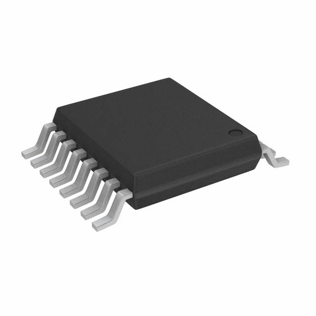
| Package / Case | 16-TSSOP |
| Package / Case [x] | 0.173 in |
| Package / Case [y] | 4.4 mm |
| Supplier Device Package | 16-TSSOP |
| Type | Decoder/Demultiplexer |
| Voltage - Supply [Max] | 5.5 V |
| Voltage - Supply [Min] | 4.5 V |
| Voltage Supply Source | Single Supply |
Pricing
Prices provided here are for design reference only. For realtime values and availability, please visit the distributors directly
| Distributor | Package | Quantity | $ | |
|---|---|---|---|---|
Description
General part information
MC74VHCT138A Series
The MC74VHCT138A is an advanced high speed CMOS 3-to-8 decoder fabricated with silicon gate CMOS technology. It achieves high speed operation similar to equivalent Bipolar Schottky TTL while maintaining CMOS low power dissipation.When the device is enabled, three Binary Select inputs (A0 - A2) determine which one of the outputs (Y0 - Y7) will go Low. When enable input E3 is held Low or either E2bar or E1bar is held High, decoding function is inhibited and all outputs go high. E3, E2bar, and E1bar inputs are provided to ease cascade connection and for use as an address decoder for memory systems.The VHCT inputs are compatible with TTL levels. This device can be used as a level converter for interfacing 3.3V to 5.0V, because they have full 5V CMOS level output swings.The VHCT138A input structures provide protection when voltages between 0V and 5.5V are applied, regardless of the supply voltage. The output structures also provide protection when VCC= 0V. These input and output structures help prevent device destruction caused by supply voltage - input/output voltage mismatch, battery backup, hot insertion, etc.
Documents
Technical documentation and resources


