Zenode.ai Logo
Beta
TOREX XC6810B42J0R-G
Integrated Circuits (ICs)

BD8316GWL-E2

Active
Rohm Semiconductor

STEP-UP AND INVERTED 2-CHANNEL DC/DC CONVERTER WITH BUILT-IN POWER MOSFET

Deep-Dive with AI

Search across all available documentation for this part.

TOREX XC6810B42J0R-G
Integrated Circuits (ICs)

BD8316GWL-E2

Active
Rohm Semiconductor

STEP-UP AND INVERTED 2-CHANNEL DC/DC CONVERTER WITH BUILT-IN POWER MOSFET

Technical Specifications

Parameters and characteristics for this part

SpecificationBD8316GWL-E2
Current - Output1 A
Frequency - Switching1.6 MHz
FunctionStep-Up/Step-Down, Step-Up
Mounting TypeSurface Mount
Number of Outputs2
Operating Temperature [Max]85 C
Operating Temperature [Min]-35 °C
Output ConfigurationPositive and Negative (Dual Rail)
Output TypeAdjustable
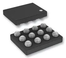
Package / CaseCSPBGA, 11-UFBGA
Supplier Device PackageUCSP50L1
Synchronous RectifierFalse
TopologyBoost, Buck-Boost
Voltage - Input (Max) [Max]5.5 V
Voltage - Input (Min) [Min]2.5 V
Voltage - Output (Max)-9 V, 18 V
Voltage - Output (Min/Fixed)-1 V, 5.5 V

Pricing

Prices provided here are for design reference only. For realtime values and availability, please visit the distributors directly

DistributorPackageQuantity$
DigikeyN/A 3310$ 1.55
NewarkEach (Supplied on Cut Tape) 1$ 2.35
10$ 1.34
25$ 1.27
50$ 1.20
100$ 1.12
250$ 0.97
500$ 0.89
1000$ 0.81

Description

General part information

BD8316GWL Series

The BD8316GWL is step-up and inverted 2-channel switching regulator with integrated internal high-side MOSFET. With wide input range from 2.5~5.5V ,it suitable for application of portable item. In addition, The small package design is ideal for miniaturizing the power supply.

Documents

Technical documentation and resources

Technical Data Sheet EN

Datasheet

Suppression Method of Switching Noise Using Linear Regulator and Low Pass Filter

Schematic Design & Verification

Considerations for Power Inductors Used for Buck Converters

Schematic Design & Verification

How to Use the Thermal Resistance and Thermal Characteristics Parameters

Thermal Design

Considering Input Filter to Reduce Conducted Emissions by DCDC Converter

Schematic Design & Verification

Cutting-Edge Web Simulation Tool "ROHM Solution Simulator" Capable of Complete Circuit Verification of Power Devices and Driver ICs

White Paper

Types of Capacitors Used for Output Smoothing of Switching Regulators and their Precautions

Schematic Design & Verification

Precautions When Measuring the Rear of the Package with a Thermocouple

Thermal Design

Thermal Resistance

Thermal Design

Factory Information

Manufacturing Data

What Is Thermal Design

Thermal Design

Power Supply Sequence Circuit with General Purpose Power Supply IC

Schematic Design & Verification

Considering Polarity of Power Inductor to Reduce Radiated Emission of DC-DC converter

Schematic Design & Verification

Heat Dissipation Effect of Thermal Via in Exposed Pad Type Package

Thermal Design

Capacitor Calculation for Buck converter IC

Schematic Design & Verification

PCB Layout Essential Check sheet for Switching Regulator

Schematic Design & Verification

Measurement Method for Phase Margin with Frequency Response Analyzer (FRA)

Schematic Design & Verification

The Important Points of Multi-layer Ceramic Capacitor Used in Buck Converter circuit

Schematic Design & Verification

Phase Compensation Design for Current Mode Buck Converter

Schematic Design & Verification

How to Use the Two-Resistor Model

Thermal Design

θ<sub>JC</sub> and Ψ<sub>JT</sub>

Thermal Design

PCB Layout Techniques of Buck Converter

Schematic Design & Verification

Two-Resistor Model for Thermal Simulation

Thermal Design

Calculation of Power Dissipation in Switching Circuit

Schematic Design & Verification

Overview of ROHM's Simulation Models(for ICs and Discrete Semiconductors)

Technical Article

Efficiency of Buck Converter

Schematic Design & Verification

Method for Calculating Junction Temperature from Transient Thermal Resistance Data

Thermal Design

BD8316GWL SPICE Modeling Report

Models

Resistor Value Table to set Output Voltage of Buck Converter IC

Schematic Design & Verification

BD8316GWL-EVK-001 User’s Guide

User's Guide

BD8316GWL Package Information

Package Information

Inductor Calculation for Buck converter IC

Schematic Design & Verification

Impedance Characteristics of Bypass Capacitor

Schematic Design & Verification

Solder Joint Rate and Thermal Resistance of Exposed Pad

Thermal Design

Three Steps for Successful Design of DC-DC Converters

White Paper

θ<sub>JA</sub> and Ψ<sub>JT</sub>

Thermal Design

Step-down DC-DC converter PCB layout EMC Design guide

Schematic Design & Verification

Design Guide and Example of Stencil for Exposed Pad

Thermal Design

Snubber Circuit for Buck Converter IC

Schematic Design & Verification

Judgment Criteria of Thermal Evaluation

Thermal Design

Compliance with the ELV directive

Environmental Data

PCB Layout Thermal Design Guide

Thermal Design

Five Steps for Successful Thermal Design of IC

White Paper

Precautions for PCB Layout Regarding Common Mode Filters

Technical Article

Basics of Thermal Resistance and Heat Dissipation

Thermal Design