8735BYI-01LF
ObsoleteLOW SKEW, 1-TO-5, DIFFERENTIAL-TO-3.3V LVPECL/ECL FANOUT BUFFER
Deep-Dive with AI
Search across all available documentation for this part.

8735BYI-01LF
ObsoleteLOW SKEW, 1-TO-5, DIFFERENTIAL-TO-3.3V LVPECL/ECL FANOUT BUFFER
Deep-Dive with AI
Technical Specifications
Parameters and characteristics for this part
| Specification | 8735BYI-01LF |
|---|---|
| Differential - Input:Output [custom] | True |
| Differential - Input:Output [custom] | True |
| Divider/Multiplier | Yes/No |
| Input | LVDS, LVPECL, LVHSTL, HCSL |
| Mounting Type | Surface Mount |
| Number of Circuits | 1 |
| Operating Temperature [Max] | 85 °C |
| Operating Temperature [Min] | -40 °C |
| Output | LVPECL |
| Package / Case | 32-LQFP |
| PLL | Yes with Bypass |
| Ratio - Input:Output | 2:5 |
| Supplier Device Package | 32-TQFP (7x7) |
| Voltage - Supply [Max] | 3.465 V |
| Voltage - Supply [Min] | 3.135 V |
Pricing
Prices provided here are for design reference only. For realtime values and availability, please visit the distributors directly
| Distributor | Package | Quantity | $ | |
|---|---|---|---|---|
Description
General part information
8735BI-01 Series
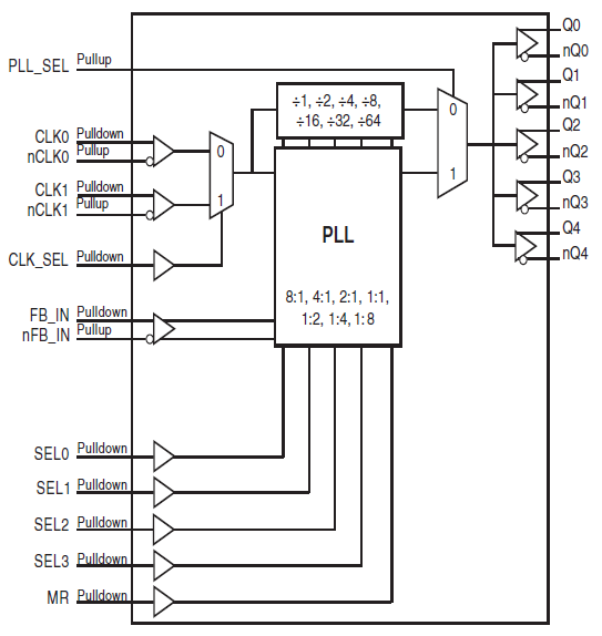
The 8735BI-01 is a highly versatile 1:5 differential- to-3.3V LVPECL clock generator. The 8735BI-01 has a fully integrated PLL and can be configured as zero delay buffer, multiplier, or divider, and has an output frequency range of 31.25MHz to 700MHz. The reference divider, feedback divider, and output divider are each programmable, thereby allowing for the following output-to-input frequency ratios: 8:1, 4:1, 2:1, 1:1, 1:2, 1:4, and 1:8. The external feedback allows the device to achieve "zero delay" between the input clock and the output clocks. The PLL_SEL pin can be used to bypass the PLL for system test and debug purposes. In bypass mode, the reference clock is routed around the PLL and into the internal output dividers.
Documents
Technical documentation and resources


