Deep-Dive with AI
Search across all available documentation for this part.

Deep-Dive with AI
Technical Specifications
Parameters and characteristics for this part
| Specification | SN74LVT8986GGV |
|---|---|
| Logic Type | Linking Addressable Scan Ports |
| Mounting Type | Surface Mount |
| Operating Temperature [Max] | 85 °C |
| Operating Temperature [Min] | -40 °C |
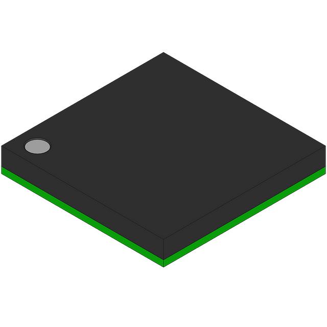
| Package / Case | 64-LFBGA |
| Supplier Device Package | 64-BGA MICROSTAR (8x8) |
| Supply Voltage [Max] | 3.6 V |
| Supply Voltage [Min] | 2.7 VDC |
Pricing
Prices provided here are for design reference only. For realtime values and availability, please visit the distributors directly
| Distributor | Package | Quantity | $ | |
|---|---|---|---|---|
Description
General part information
SN74LVT8986 Series
The 'LVT8986 linking addressable scan ports (LASPs) are members of the TI family of IEEE Std 1149.1 (JTAG) scan-support products. The scan-support product family facilitates testing of fully boundary-scannable devices. The LASP applies linking shadow protocols through the test access port (TAP) to extend scan access to the system level and divide scan chains at the board level.
The LASP consists of a primary TAP for interfacing to the backplane IEEE Std 1149.1 serial-bus signals (PTDI, PTMS, PTCK, PTDO,PRTST) and three secondary TAPs for interfacing to the board-level IEEE Std 1149.1 serial-bus signals. Each secondary TAP consists of signals STDIx, STMSx, STCKx, STDOx, andSTRSTx. Conceptually, the LASP is a gateway device that can be used to connect a set of primary TAP signals to a set of secondary TAP signals — for example, to interface backplane TAP signals to a board-level TAP. The LASP provides all signal buffering that might be required at these two interfaces. Primary-to-secondary TAP connections can be configured with the help of linking shadow protocol or protocol bypass (BYP5-BYP0) inputs.
Most operations of the LASP are synchronous to the primary test clock (PTCK) input. PTCK always is buffered directly onto the secondary test clock (STCK2-STCK0) outputs. Upon power up of the device, the LASP assumes a condition in which the primary TAP is disconnected from the secondary TAPs (unless the bypass signals are used, as shown in Function Tables 1 and 2). This reset condition also can be entered by asserting the primary test reset (PTRST) input or by using the linking shadow protocol.PTRSTalways is buffered directly onto the secondary test reset (STRST2-STRST0) outputs, ensuring that the LASP and its associated secondary TAPs can be reset simultaneously. The primary test data output (PTDO) can be configured to receive secondary test data inputs (STDI2-STDI0). Secondary test data outputs (STDO2-STDO0) can be configured to receive either the primary test data input (PTDI), STDI2-STDI0, or the cascade test data input (CTDI). Cascade test data output (CTDO) can be configured to receive either of STDI2-STDI0, or CTDI. CTDI and CTDO facilitate cascading multiple LASPs, which is explained in the latter part of this section. Similarly, secondary test-mode select (STMS2-STMS0) outputs can be configured to receive the primary test-mode select (PTMS) input. When any secondary TAP is disconnected, its respective STDO is at high impedance. Upon disconnecting the secondary TAP, the corresponding STMS holds its last low or high level, allowing the secondary TAP to be held in its last stable state.
Documents
Technical documentation and resources
No documents available


