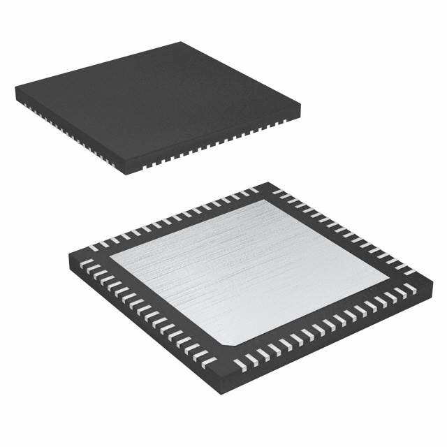
MAX5877EGK+D
Active14-BIT, 250MSPS, HIGH-DYNAMIC-PERFORMANCE, DUAL DAC WITH LVDS INPUTS
Deep-Dive with AI
Search across all available documentation for this part.

MAX5877EGK+D
Active14-BIT, 250MSPS, HIGH-DYNAMIC-PERFORMANCE, DUAL DAC WITH LVDS INPUTS
Deep-Dive with AI
Technical Specifications
Parameters and characteristics for this part
| Specification | MAX5877EGK+D |
|---|---|
| Architecture | Current Steering |
| Data Interface | Parallel |
| Differential Output | True |
| INL/DNL (LSB) | 0.5 LSB, 0.2 LSB |
| Mounting Type | Surface Mount |
| Number of Bits | 14 |
| Operating Temperature [Max] | 85 °C |
| Operating Temperature [Min] | -40 C |
| Output Type | Current - Unbuffered |
| Package / Case | 68-VFQFN Exposed Pad |
| Reference Type | Internal, External |
| Supplier Device Package | 68-QFN |
| Supplier Device Package [x] | 10 |
| Supplier Device Package [y] | 10 |
| Voltage - Supply, Analog [Max] | 3.465 V, 1.89 V |
| Voltage - Supply, Analog [Min] | 1.71 V, 3.135 V |
| Voltage - Supply, Digital [Max] | 1.89 V, 3.465 V |
| Voltage - Supply, Digital [Min] | 1.71 V, 3.135 V |
Pricing
Prices provided here are for design reference only. For realtime values and availability, please visit the distributors directly
| Distributor | Package | Quantity | $ | |
|---|---|---|---|---|
| Digikey | N/A | 0 | $ 42.10 | |
| 1470 | $ 42.10 | |||
| Tube | 1 | $ 34.50 | ||
| 10 | $ 31.82 | |||
| 30 | $ 30.39 | |||
| 120 | $ 27.17 | |||
| 270 | $ 25.92 | |||
Description
General part information
MAX5877 Series
The MAX5877 is an advanced 14-bit, 250Msps, dual digital-to-analog converter (DAC). This DAC meets the demanding performance requirements of signal synthesis applications found in wireless base stations and other communications applications. Operating from +3.3V and +1.8V supplies, this dual DAC offers exceptional dynamic performance such as 75dBc spurious-free dynamic range (SFDR) at fOUT= 16MHz and supports update rates of 250Msps, with a power dissipation of only 287mW.The MAX5877 utilizes a current-steering architecture that supports a 2mA to 20mA full-scale output current range, and allows a 0.1VP-Pto 1VP-Pdifferential output voltage swing. The device features an integrated +1.2V bandgap reference and control amplifier to ensure high-accuracy and low-noise performance. A separate reference input (REFIO) allows for the use of an external reference source for optimum flexibility and improved gain accuracy.The clock inputs of the MAX5877 accept both LVDS and LVPECL-compatible voltage levels. The device features an interleaved data input that allows a single LVDS bus to support both DACs. The MAX5877 is available in a 68-pin QFN package with an exposed pad (EP) and is specified for the extended temperature range (-40°C to +85°C).Refer to theMAX5876andMAX5878data sheets for pin-compatible 12-bit and 16-bit versions of the MAX5877, respectively. Refer to theMAX5874data sheet for a CMOS-compatible version of the MAX5877.See a parametric table of the complete family of pin-compatible 12-/14-/16-bit high-speed DACs.ApplicationsAutomated Test Equipment (ATE)Base Stations: Single-/Multicarrier UMTS, CDMA, GSMCable Modem Termination Systems (CMTS)Communications: Fixed Broadband Wireless Access, Point-to-Point MicrowaveDirect Digital Synthesis (DDS)Instrumentation
Documents
Technical documentation and resources


