Deep-Dive with AI
Search across all available documentation for this part.

Deep-Dive with AI
Technical Specifications
Parameters and characteristics for this part
| Specification | SN74GTLP2033GQLR |
|---|---|
| Logic Type | LVTTL-TO-GTLP Adjustable-Edge-Rate Registered Transceiver |
| Mounting Type | Surface Mount |
| Number of Bits | 8 |
| Operating Temperature [Max] | 85 °C |
| Operating Temperature [Min] | -40 °C |
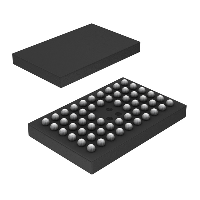
| Package / Case | 56-VFBGA |
| Supplier Device Package | 56-BGA Microstar Junior (7x4.5) |
| Supply Voltage [Max] | 3.45 V |
| Supply Voltage [Min] | 3.15 V |
Pricing
Prices provided here are for design reference only. For realtime values and availability, please visit the distributors directly
| Distributor | Package | Quantity | $ | |
|---|---|---|---|---|
Description
General part information
SN74GTLP2033 Series
The SN74GTLP2033 is a high-drive, 8-bit, three-wire registered transceiver that provides inverted LVTTL-to-GTLP and GTLP-to-LVTTL signal-level translation. The device allows for transparent, latched, and flip-flop modes of data transfer with separate LVTTL input and LVTTL output pins, which provides a feedback path for control and diagnostics monitoring, the same functionality as the SN74FB2033. The device provides a high-speed interface between cards operating at LVTTL logic levels and a backplane operating at GTLP signal levels. High-speed (about three times faster than standard LVTTL or TTL) backplane operation is a direct result of GTLP's reduced output swing (<1 V), reduced input threshold levels, improved differential input, OEC™ circuitry, and TI-OPC™ circuitry. Improved GTLP OEC and TI-OPC circuits minimize bus-settling time and have been designed and tested using several backplane models. The high drive allows incident-wave switching in heavily loaded backplanes with equivalent load impedance down to 11.
GTLP is the Texas Instruments derivative of the Gunning Transceiver Logic (GTL) JEDEC standard JESD 8-3. The ac specification of the SN74GTLP2033 is given only at the preferred higher noise-margin GTLP, but the user has the flexibility of using this device at either GTL (VTT= 1.2 V and VREF= 0.8 V) or GTLP (VTT= 1.5 V and VREF= 1 V) signal levels. For information on using GTLP devices in FB+/BTL applications, refer to TI application reports,Texas Instruments GTLP Frequently Asked Questions, literature number SCEA019, andGTLP in BTL Applications, literature number SCEA017.
Normally, the B port operates at GTLP signal levels. The A-port and control inputs operate at LVTTL logic levels, but are 5-V tolerant and can be directly driven by TTL or 5-V CMOS devices. VREFis the B-port differential input reference voltage.
Documents
Technical documentation and resources


