RC21008B001GND#BB0
ActiveVERSACLOCK 7 PROGRAMMABLE CLOCK GENERATOR FAMILY
Deep-Dive with AI
Search across all available documentation for this part.

RC21008B001GND#BB0
ActiveVERSACLOCK 7 PROGRAMMABLE CLOCK GENERATOR FAMILY
Deep-Dive with AI
Technical Specifications
Parameters and characteristics for this part
| Specification | RC21008B001GND#BB0 |
|---|---|
| Differential - Input:Output | True |
| Divider/Multiplier | Yes/No |
| Frequency - Max [Max] | 650 MHz, 200 MHz |
| Input | HCSL, LVCMOS, LVDS, CML, Crystal, LVPECL |
| Mounting Type | Surface Mount |
| Number of Circuits | 1 |
| Operating Temperature [Max] | 85 C |
| Operating Temperature [Min] | -40 ¯C |
| Output | LVDS, LP-HCSL, LVCMOS |
| Package / Case | 40-VFQFN Exposed Pad |
| PLL | True |
| Ratio - Input:Output [custom] | 3:8 |
| Supplier Device Package | 40-VFQFPN (5x5) |
| Type | Clock Generator |
| Voltage - Supply [Max] | 2.625 V, 3.465 V, 1.89 V |
| Voltage - Supply [Min] | 1.71 V, 2.375 V, 3.135 V |
Pricing
Prices provided here are for design reference only. For realtime values and availability, please visit the distributors directly
| Distributor | Package | Quantity | $ | |
|---|---|---|---|---|
| Digikey | N/A | 0 | $ 8.53 | |
Description
General part information
RC210 Series
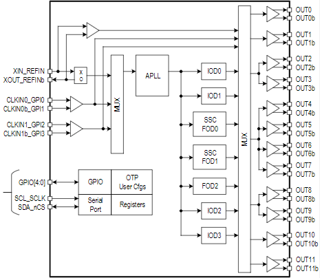
The RC21xxxB (RC21012B and RC21008B) is a member of Renesas's VersaClock®7 programmable clock generator family. It is intended for high-performance computers, data communications, and industrial applications, designed to be placed immediately adjacent to a PHY, switch, ASIC or FPGA that requires several reference clocks with jitter performance 150fs typical RMS.
Up to 27 configurations reusable across multiple designs may be stored in on-chip One-Time Programmable (OTP) memory or external I2C EEPROM. Redundant input is available for backup and used as a reference clock where needed.
Documents
Technical documentation and resources


