Deep-Dive with AI
Search across all available documentation for this part.

Deep-Dive with AI
Technical Specifications
Parameters and characteristics for this part
| Specification | SN74LS155ADRG4 |
|---|---|
| Circuit | 1 x 2:4 |
| Current - Output High, Low [custom] | 400 µA |
| Current - Output High, Low [custom] | 8 mA |
| Independent Circuits | 2 |
| Mounting Type | Surface Mount |
| Operating Temperature [Max] | 70 °C |
| Operating Temperature [Min] | 0 °C |
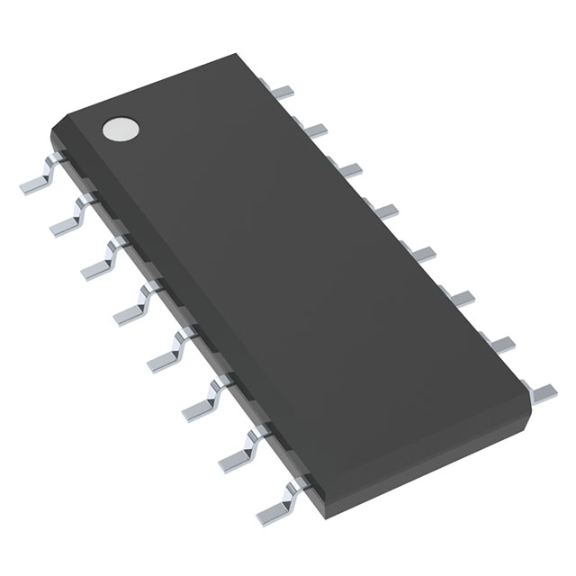
| Package / Case | 16-SOIC |
| Package / Case [x] | 0.154 in |
| Package / Case [y] | 3.9 mm |
| Supplier Device Package | 16-SOIC |
| Type | Decoder/Demultiplexer |
| Voltage - Supply [Max] | 5.25 V |
| Voltage - Supply [Min] | 4.75 V |
| Voltage Supply Source | Single Supply |
Pricing
Prices provided here are for design reference only. For realtime values and availability, please visit the distributors directly
| Distributor | Package | Quantity | $ | |
|---|---|---|---|---|
| Digikey | Tape & Reel (TR) | 2500 | $ 0.62 | |
| 5000 | $ 0.59 | |||
| 12500 | $ 0.57 | |||
Description
General part information
SN74LS155A Series
These monolithic transistor-transistor-logic (TTL) circuits feature dual 1-line-to-4-line demultiplexers with individual strobes and common binary-address inputs in a single 16-pin package. When both sections are enabled by the strobes, the common binary-address inputs sequentially select and route associated input data to the appropriate output of each section. The individual strobes permit activating or inhibiting each of the 4-bit sections as desired. Data applied to input 1C is inverted at its outputs and data applied at 2C\ is not inverted through its outputs. The inverter following the 1C data input permits use as a 3-to-8-line decoder or 1-to-8-line demultiplexer without external gating. Input clamping diodes are provided on all of these circuits to minimize transmission-line effects and simplify system design.
These monolithic transistor-transistor-logic (TTL) circuits feature dual 1-line-to-4-line demultiplexers with individual strobes and common binary-address inputs in a single 16-pin package. When both sections are enabled by the strobes, the common binary-address inputs sequentially select and route associated input data to the appropriate output of each section. The individual strobes permit activating or inhibiting each of the 4-bit sections as desired. Data applied to input 1C is inverted at its outputs and data applied at 2C\ is not inverted through its outputs. The inverter following the 1C data input permits use as a 3-to-8-line decoder or 1-to-8-line demultiplexer without external gating. Input clamping diodes are provided on all of these circuits to minimize transmission-line effects and simplify system design.
Documents
Technical documentation and resources
No documents available


