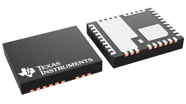
CSD95411RRB
Active65-A PEAK CONTINUOUS CURRENT SYNCHRONOUS BUCK NEXFET™ POWER STAGE
Deep-Dive with AI
Search across all available documentation for this part.

CSD95411RRB
Active65-A PEAK CONTINUOUS CURRENT SYNCHRONOUS BUCK NEXFET™ POWER STAGE
Deep-Dive with AI
Technical Specifications
Parameters and characteristics for this part
| Specification | CSD95411RRB |
|---|---|
| Applications | Synchronous Buck Converters |
| Current - Peak Output | 65 A |
| Fault Protection | Shoot-Through |
| Features | Bootstrap Circuit |
| Interface | PWM |
| Load Type | Inductive |
| Mounting Type | Surface Mount |
| Operating Temperature [Max] | 150 °C |
| Operating Temperature [Min] | -55 °C |
| Package / Case | 41-PowerTFQFN |
| Supplier Device Package | 41-VQFN-CLIP |
| Technology | Power MOSFET |
Pricing
Prices provided here are for design reference only. For realtime values and availability, please visit the distributors directly
| Distributor | Package | Quantity | $ | |
|---|---|---|---|---|
| Digikey | Bulk | 2500 | $ 2.14 | |
| LCSC | Piece | 1 | $ 7.07 | |
| 10 | $ 6.90 | |||
| 30 | $ 6.79 | |||
| 100 | $ 6.68 | |||
| Texas Instruments | LARGE T&R | 1 | $ 3.45 | |
| 100 | $ 3.03 | |||
| 250 | $ 2.12 | |||
| 1000 | $ 1.71 | |||
Description
General part information
CSD95411 Series
The CSD95411 NexFET™ power stage is a highly optimized design for use with a high-power, high-density synchronous buck converter. This device integrates the driver IC and power MOSFETs to complete the power stage switching function. This combination produces high-current, high-efficiency, and high-speed switching capability in a small 5-mm × 6-mm outline package. The power stage also integrates the accurate current sensing and temperature sensing functionality to simplify system design and improve accuracy. The optimized PCB footprint helps reduce design time and simplify the completion of the overall system design.
The CSD95411 NexFET™ power stage is a highly optimized design for use with a high-power, high-density synchronous buck converter. This device integrates the driver IC and power MOSFETs to complete the power stage switching function. This combination produces high-current, high-efficiency, and high-speed switching capability in a small 5-mm × 6-mm outline package. The power stage also integrates the accurate current sensing and temperature sensing functionality to simplify system design and improve accuracy. The optimized PCB footprint helps reduce design time and simplify the completion of the overall system design.
Documents
Technical documentation and resources


