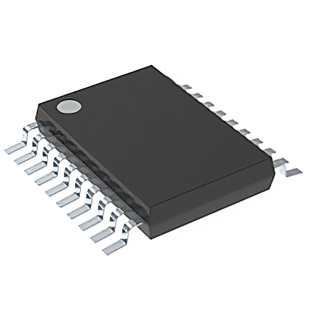
SN74LVTH540PWR
Active8-CH, 2.7-V TO 3.6-V INVERTERS WITH BUS-HOLD, TTL-COMPATIBLE CMOS INPUTS AND 3-STATE OUTPUTS
Deep-Dive with AI
Search across all available documentation for this part.

SN74LVTH540PWR
Active8-CH, 2.7-V TO 3.6-V INVERTERS WITH BUS-HOLD, TTL-COMPATIBLE CMOS INPUTS AND 3-STATE OUTPUTS
Deep-Dive with AI
Technical Specifications
Parameters and characteristics for this part
| Specification | SN74LVTH540PWR |
|---|---|
| Current - Output High, Low [custom] | 64 mA |
| Current - Output High, Low [custom] | 32 mA |
| Logic Type | Inverting, Buffer |
| Mounting Type | Surface Mount |
| Number of Bits per Element | 8 |
| Number of Elements | 1 |
| Operating Temperature [Max] | 85 °C |
| Operating Temperature [Min] | -40 °C |
| Output Type | 3-State |
| Package / Case | 20-TSSOP |
| Package / Case [x] | 0.173 in |
| Package / Case [y] | 4.4 mm |
| Supplier Device Package | 20-TSSOP |
| Voltage - Supply [Max] | 3.6 V |
| Voltage - Supply [Min] | 2.7 V |
Pricing
Prices provided here are for design reference only. For realtime values and availability, please visit the distributors directly
| Distributor | Package | Quantity | $ | |
|---|---|---|---|---|
| Digikey | Cut Tape (CT) | 1 | $ 2.67 | |
| 10 | $ 1.72 | |||
| 25 | $ 1.47 | |||
| 100 | $ 1.20 | |||
| 250 | $ 1.06 | |||
| 500 | $ 0.98 | |||
| 1000 | $ 0.91 | |||
| Digi-Reel® | 1 | $ 2.67 | ||
| 10 | $ 1.72 | |||
| 25 | $ 1.47 | |||
| 100 | $ 1.20 | |||
| 250 | $ 1.06 | |||
| 500 | $ 0.98 | |||
| 1000 | $ 0.91 | |||
| Tape & Reel (TR) | 2000 | $ 0.80 | ||
| 6000 | $ 0.77 | |||
| 10000 | $ 0.74 | |||
| Texas Instruments | LARGE T&R | 1 | $ 1.32 | |
| 100 | $ 1.09 | |||
| 250 | $ 0.78 | |||
| 1000 | $ 0.59 | |||
Description
General part information
SN74LVTH540 Series
These octal buffers/drivers are designed specifically for low-voltage (3.3-V) VCCoperation, but with the capability to provide a TTL interface to a 5-V system environment.
The ’LVTH540 devices are ideal for driving bus lines or buffer memory address registers. These devices feature inputs and outputs on opposite sides of the package that facilitate printed circuit board layout.
The 3-state control gate is a 2-input AND gate with active-low inputs so that if either output-enable (OE1\ or OE2\) input is high, all outputs are in the high-impedance state.
Documents
Technical documentation and resources


