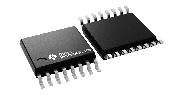
CD14538BPWR
ActiveMONOSTABLE MULTIVIBRATOR DUAL-ELEMENT -55°C 125°C 16-PIN TSSOP T/R
Deep-Dive with AI
Search across all available documentation for this part.

CD14538BPWR
ActiveMONOSTABLE MULTIVIBRATOR DUAL-ELEMENT -55°C 125°C 16-PIN TSSOP T/R
Deep-Dive with AI
Technical Specifications
Parameters and characteristics for this part
| Specification | CD14538BPWR |
|---|---|
| Current - Output High, Low [custom] | 6.8 mA |
| Current - Output High, Low [custom] | 6.8 mA |
| Independent Circuits | 2 |
| Logic Type | Monostable |
| Mounting Type | Surface Mount |
| Operating Temperature [Max] | 125 °C |
| Operating Temperature [Min] | -55 °C |
| Package / Case | 16-TSSOP |
| Package / Case [x] | 0.173 in |
| Package / Case [y] | 4.4 mm |
| Propagation Delay | 100 ns |
| Schmitt Trigger Input | True |
| Supplier Device Package | 16-TSSOP |
| Voltage - Supply [Max] | 18 V |
| Voltage - Supply [Min] | 3 V |
Pricing
Prices provided here are for design reference only. For realtime values and availability, please visit the distributors directly
| Distributor | Package | Quantity | $ | |
|---|---|---|---|---|
| Digikey | Cut Tape (CT) | 1 | $ 0.54 | |
| 10 | $ 0.47 | |||
| 25 | $ 0.44 | |||
| 100 | $ 0.35 | |||
| 250 | $ 0.32 | |||
| 500 | $ 0.27 | |||
| 1000 | $ 0.21 | |||
| Digi-Reel® | 1 | $ 0.54 | ||
| 10 | $ 0.47 | |||
| 25 | $ 0.44 | |||
| 100 | $ 0.35 | |||
| 250 | $ 0.32 | |||
| 500 | $ 0.27 | |||
| 1000 | $ 0.21 | |||
| Tape & Reel (TR) | 2000 | $ 0.19 | ||
| 6000 | $ 0.18 | |||
| 10000 | $ 0.17 | |||
| 50000 | $ 0.16 | |||
| Texas Instruments | LARGE T&R | 1 | $ 0.35 | |
| 100 | $ 0.24 | |||
| 250 | $ 0.18 | |||
| 1000 | $ 0.12 | |||
Description
General part information
CD14538B Series
CD14538B dual precision monostable multivibrator provides stable retriggerable/resettable one-shot operation for any fixed-voltage timing application.
An external resistor (RX) and an external capacitor (CX) control the timing and accuracy for the circuit. Adjustment of RXand CXprovides a wide range of output pulse widths from the Q and Q\ terminals. The time delay from trigger input to output transition (trigger propagation delay) and the time delay from reset input to output transition (reset propagation delay) are independent of RXand CX. Precision control of output pulse widths is achieved through linear CMOS techniques.
Leading-edge-triggering (+TR) and trailing-edge-triggering (-TR) inputs are provided for triggering from either edge of an input pulse. An unused +TR input should be tied to VSS. An unused -TR input should be tied to VDD. A RESET (on low level) is provided for immediate termination of the output pulse or to prevent output pulses when power is turned on. An unused RESET input should be tied to VDD. However, if an entire section of the CD14538B is not used, its inputs must be tied to either VDDor VSS. See Table 1.
Documents
Technical documentation and resources


